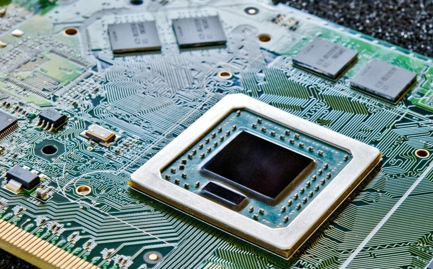
HDI 1+N+1 vs 2+N+2: Microvia Stackup Comparison
Reading the Notation
The numbers in an HDI stackup describe how many build up layers sit on each side of a conventional core. In 1+N+1 there is one microvia layer on the top and one on the bottom, so a via can reach the first inner layer only. In 2+N+2 there are two build up layers on each side, which means a via can also land on the second inner layer, and the board can route on twice as many fine pitch layers. The N is the core, a normal mechanically drilled laminate that carries the power, ground and coarse routing. Everything that distinguishes the two structures happens in the thin dielectric layers bonded on the outside.
Routing Density and Escape Rate
The practical meaning of the stackup is how many traces can escape from a dense component. A 0.4 mm pitch BGA on a 1+N+1 board typically escapes in two directions on the top layer and then drops through a microvia to the first inner layer, which is where the density bottleneck sits. Adding a second build up layer gives another routing plane within the microvia reach, which roughly doubles the escape channels. That is why a design that fails to route at 1+N+N almost always passes at 2+N+2 without changing the ball pitch or the layer count of the core.

Microvia Formation and Stacking
Both structures are built with laser drilled microvias, but the allowable arrangements differ. In 1+N+1 the microvias normally land directly on the core, so they are single level and staggered or offset connections are not required. In 2+N+2 the second level via may be stacked directly on the first, or staggered so that it lands on a capture pad offset from the one below. Stacked vias save the most area but demand a filled and planarised via below, because a void under the next laser shot causes an unreliable connection. Staggered vias are more forgiving to build and slightly less dense. The choice between stacked and staggered is one of the main cost drivers inside the 2+N+2 family.
Reliability and Thermal Cycling
Each microvia adds a plated barrel through a thin dielectric, and reliability analysis treats those barrels as the weak point in thermal cycling. A 1+N+1 board has the shortest and simplest via path from surface to inner layer, so it generally shows the longest fatigue life. A 2+N+2 board has more barrels in series when the vias are stacked, and the second level sits over filled resin rather than solid laminate, so the coefficient of thermal expansion mismatch is more complex. Copper filled and planarised vias substantially improve the result, which is why high reliability products that need 2+N+2 usually specify copper fill rather than conductive paste.

Fabrication Limits and Yield
Every additional build up layer adds lamination cycles, and each cycle adds registration error and handling risk. A 2+N+2 board goes through two sequential laminations on each side, with laser drilling and plating in between, so the number of process steps roughly doubles compared with 1+N+1. The dielectric thickness of the outer layers has to be kept thin to allow the microvia aspect ratio, which constrains the impedance options and the copper weight. Those constraints are the reason a stackup that looks simple on a drawing can be difficult to build, and why the fabricator should review the construction before the design is frozen.
Where the Cost Goes
Lamination cycles. Two build up layers mean twice the press cycles, and press time is expensive. Laser drilling. The hole count multiplies, and stacked vias need filled copper rather than paste. Registration. Tighter layer to layer tolerance adds inspection and can lower yield. Material. Thin prepreg and copper foil for the outer layers carry a premium. Panel size. Distortion after multiple cycles limits how large a panel can be used, which affects the unit price. As a rule of thumb 2+N+2 costs meaningfully more than 1+N+1, and the gap widens if stacked copper filled vias are specified.
Choosing Between Them
Start with the escape count. If a 1+N+1 stackup lets every dense device break out with acceptable layer usage, there is no reason to pay for a second build up layer. Move to 2+N+2 when the ball pitch is very fine, the layer count of the core would otherwise grow, or the board needs shielding and ground planes close to the surface. In many designs a hybrid works best: 1+N+1 on the side with the dense digital device and a conventional multilayer on the other side, which keeps the cost of the build up to one face. Verify the choice with a stackup review rather than a template, because the same nominal notation can hide very different dielectric thicknesses.
Stackup decisions belong with the rest of the electrical design. Read how HDI boards are built in PCB manufacturing, apply the routing rules in PCB design and layout, and review the design and manufacturing considerations before release. A prototype PCB assembly build with a cross section check confirms the stackup performs as intended.
FAQ
What does N mean in 2+N+2? It is the conventional core, mechanically drilled, carrying power, ground and coarse routing between the two build up layers.
Is 2+N+2 always better than 1+N+1? No. It offers more routing density but costs more and adds lamination cycles, so use it only when the escape rate requires it.
Should microvias be stacked or staggered? Stacked saves area but needs copper filled and planarised vias; staggered is easier to build and is preferred when the density allows.
Does the stackup affect reliability? Yes. More microvias in series reduce thermal fatigue life, which is why copper fill and careful design matter in 2+N+2 boards.
Conclusion
1+N+1 gives one microvia layer per side and is the cheaper, more robust choice whenever the escape count allows it. 2+N+2 doubles the fine pitch routing capacity at the cost of extra lamination cycles, tighter registration and the question of how to stack the vias. Decide from the ball pitch and escape analysis, prefer single level build up where it routes, and confirm the construction with the fabricator in 2026 before the design is frozen.