Communication Module PCB Guide: Materials, Design, and Reliability
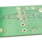
A communication module seems small, but its circuit board must coordinate RF transceivers, baseband processors, power management, and interface components. A communication module PCB is the physical foundation of that system, providing stable impedance, clean power, and dependable assembly quality across temperature and usage conditions.
Base Material and Dimensional Stability
Most communication module boards use glass-fiber reinforced epoxy laminate, commonly known as FR-4. The material provides good electrical insulation and mechanical strength while maintaining dimensional stability across the operating temperature range of typical modules. The woven glass structure supports components through reflow and protects fine traces during normal handling.
Copper Traces and Controlled Impedance
Copper foil forms the conductive network for signal routing and power distribution. After imaging and etching, trace widths and spacing are held within tight tolerances so high-speed interfaces keep their target impedance. Main traces handle power and ground returns, while fine branch traces connect small RF and digital components without creating unnecessary capacitance or inductance.<

/p>
Precision Routing, Fiducials, and Assembly Accuracy
Communication modules are assembled automatically in high volume, so the board outline and reference marks must be extremely accurate. CNC routing creates clean edges with controlled tolerances, and fiducial marks give placement machines a stable reference. Locating holes and edge features help ensure that connectors and shields fit correctly during final assembly.
Solder Mask and Surface Finish
Liquid photoimageable solder mask protects the board from unintended solder bridges, moisture, and oxidation. Pads receive finishes such as ENIG or HASL depending on component pitch and reliability needs. ENIG provides a flat, corrosion-resistant surface for fine-pitch modules, while HASL may be used where lower cost is more important.
Test Points and Edge Connections
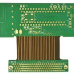
Test points allow automated probes to verify continuity, insulation, and key electrical signals during production. Some modules add plated edge fingers with hard gold for repeated insertion into sockets or card connectors. Both features help manufacturers catch defects early and make field service more practical.
Designing a Reliable Communication Module Board
Reliability starts before production. RF and high-speed traces should use continuous reference planes, minimal vias, and clear component placement around sensitive circuits. A DFM review can confirm that the stackup, minimum trace width, via size, and finish are suitable for the target frequency. RF and high-speed PCB design support is especially useful when the module includes antennas, radios, or high-speed digital interfaces.<

/p>
When your design is ready, gopcb provides communication PCB manufacturing, SMT PCB assembly, and component procurement to build complete communication modules with controlled quality.