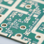
Copper Core Substrate: Fabrication and Surface Finish Choice
A copper core substrate is a middle ground between a conventional laminate and a ceramic. A metal plate carries the heat, a thin dielectric insulates it from the circuit, and the copper foil on top is processed like any other printed circuit. The result is a board that conducts heat far better than FR4 while remaining compatible with standard assembly equipment.
What a Copper Core Substrate Is For
The core exists to move heat. Where a circuit generates more thermal load than a glass reinforced laminate can spread, a metal base changes the problem from one of local hot spots to one of bulk conduction into a heat sink or a chassis. Copper is chosen over aluminium when the thermal demand is higher still, since its conductivity is roughly twice that of aluminium.
The structure is otherwise familiar. A single-sided or double-sided circuit is built on the foil above the dielectric, and the metal base provides mechanical rigidity as well as thermal mass. That rigidity is a benefit in its own right for thin assemblies and for boards that must stay flat under a connector or a mounting screw.
Substrate Material and Electrical Properties
The choice of base material influences more than thermal performance. It determines the withstand voltage the finished board can tolerate, the insulation resistance between the circuit and the metal, the dielectric constant, and the loss the dielectric introduces at high frequency. It also affects moisture absorption and how the finished product behaves under environmental regulation.
Because the metal base is conductive, the dielectric layer is what stands between the circuit and a short to the chassis. Its thickness is therefore set by the voltage the board must withstand rather than by thermal considerations alone. Thicker dielectric improves breakdown strength but adds thermal resistance, which is the central trade in metal core design. Values and their effect on impedance are discussed under PCB dielectric constant.
The Thermal Path and Why the Interface Matters
Heat passes from the component, through its attachment, through the copper foil, through the dielectric, into the metal base and out to the heat sink. Each interface adds resistance, and the dielectric layer is usually the largest single contributor despite being thin, because its thermal conductivity is low compared with metal.
That is why the practical design levers are the area of copper above each heat source, the thickness and formulation of the dielectric, and the quality of the mechanical joint between the board and whatever it is mounted on. A board with excellent internal conduction and a poor mounting interface performs no better than a modest board mounted well.
Surface Finish Options: Hot Air Solder Levelling
Hot air solder levelling is the oldest method and remains the cheapest. The board is coated with molten solder and the excess is blown off with hot air, leaving a solderable tin-lead or lead-free layer. It stores well, the process is thoroughly understood, and the equipment is available almost everywhere.
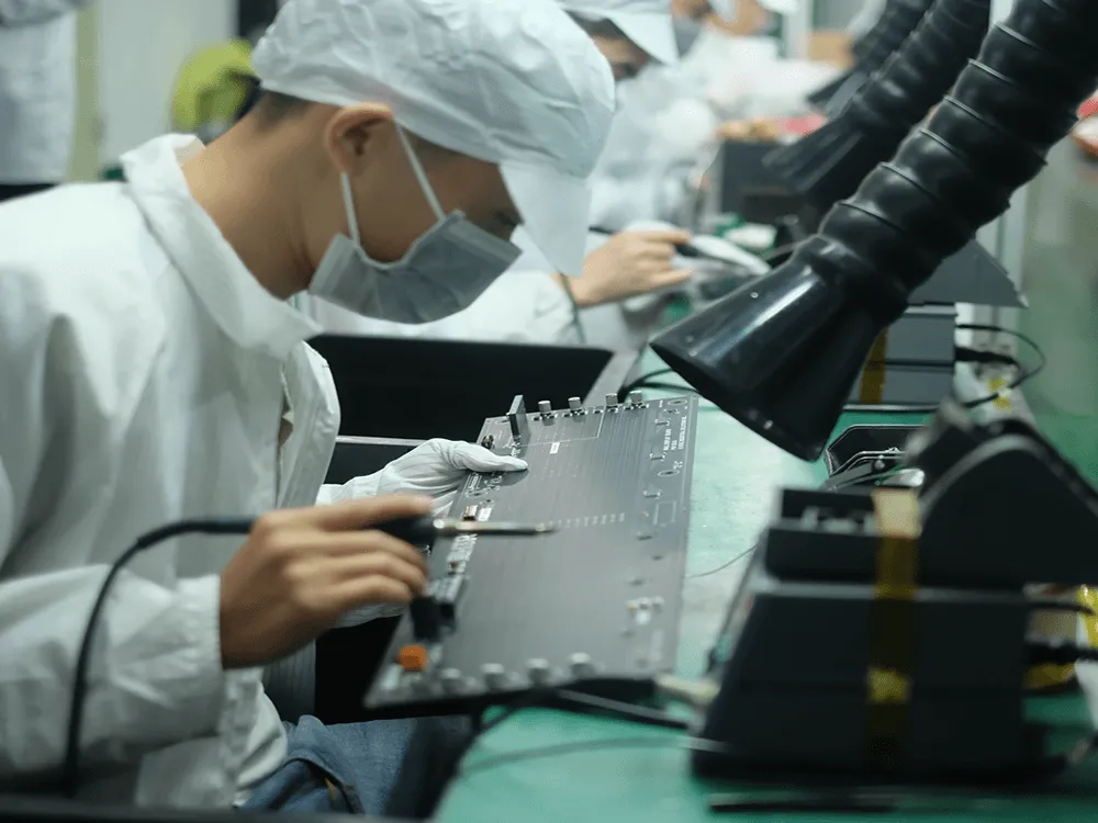
Its weakness is flatness. The coating thickness varies across the surface, and fine pitch pads, land grid arrays and ball grid arrays all suffer when the surface is not level. Very thick and very thin boards are also difficult to process, because the coating and the air knife behave differently on each. For a board with coarse geometry and a generous budget, it remains a sensible choice.
Surface Finish Options: Gold and Silver
Electroless nickel immersion gold and immersion silver produce a much flatter surface. The metal is deposited chemically rather than by molten solder, so the thickness is uniform across fine features and the pad geometry stays true to the artwork. Both finishes tolerate extended storage, with shelf lives measured in months rather than weeks under appropriate packaging.
That combination makes them suitable for contact designs, for gold and aluminium wire bonding where the gold surface is required, and for point probing during test. The costs are higher material and chemistry cost, tighter process control, and the need to manage uniformity carefully, since an uneven deposit causes the same assembly problems as any other surface defect. A fuller comparison appears in ENIG PCB finish.
Flatness, Storage Life and SMT Constraints
Flatness is the property that links finish choice to assembly yield. A solder paste stencil sits on the board surface, and any variation under the aperture changes the paste volume deposited. On a metal base board the risk is greater than on FR4, because the metal does not flex in the same way and cannot be relied upon to conform.
<img src="https://www.gopcba.com/wp-content/uploads/2021/03/bee_overlay.png" alt="Cross section of a metal core PCB showing the dielectric layer” />
Storage is the other constraint. Organic finishes have a short life and are easily contaminated, while metallic finishes survive longer but still require clean, dry packaging. Moisture absorbed before assembly causes outgassing during reflow, and on a metal core board the additional thermal mass means every reflow profile has to be established on the actual product rather than copied. Handling and bake requirements are covered in moisture sensitive devices on PCB.
Specifying a Copper Core Board
A specification should state the base metal and its thickness, the dielectric type and its breakdown rating, the copper weight on the circuit layer, the surface finish with any thickness requirement, and the flatness tolerance that assembly can accept. It should also state whether the metal base needs to be machined, anodised, or left with an exposed edge for electrical connection to the chassis.
Assembly questions follow from those decisions. Metal core boards require more heat to solder, so the profile and the tooling both change, and the practical techniques differ from those used on laminate, as described in aluminium substrate hand soldering. Settling these points before the order is placed avoids discovering them during the first production run.
How the Board Is Actually Made
Fabrication begins with the metal plate rather than with the circuit. The base is cleaned, and any holes that must pass through it are usually punched or drilled before the dielectric is applied, because machining metal after the circuit exists risks damaging the copper and the laminate bond. The dielectric is then applied as a coated sheet or a prepreg, the copper foil is laid over it, and the assembly is laminated under heat and pressure so that the resin cures and bonds to both surfaces.
The circuit is then produced by conventional imaging and etching, followed by solder mask, legend, surface finish and profiling. Two steps differ noticeably from FR4. Drilling metal produces burrs and heat, and the tooling must be selected for a material that behaves quite differently from a glass laminate, with aluminium tending to gall and copper requiring more cutting force. Profiling is similar, since routing or punching a metal base consumes tooling faster and produces an edge that may need deburring before the board can be handled safely.
FAQ
When should a copper core be used instead of aluminium? When the thermal load exceeds what an aluminium base can dissipate, or when the coefficient of thermal expansion of copper matches the assembly better. Copper costs more and weighs more, so the justification is thermal or mechanical.
What is the main weakness of hot air solder levelling? Surface flatness. The process leaves an uneven coating that causes paste volume variation on fine pitch pads, which is why area array and fine pitch assemblies normally use a chemically deposited finish instead.
Does the dielectric thickness affect signal behaviour? Yes. It sets the impedance of the traces above it as well as the breakdown voltage, so electrical and safety requirements have to be balanced against the thermal resistance the design can tolerate.