



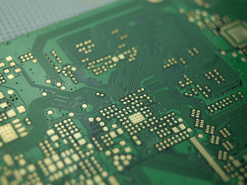
Photoresist Developing in PCB Fabrication: Control and Defects
Imaging is the step where a design stops being data and becomes a pattern on copper foil, and photoresist developing is where that pattern first becomes visible. Everything that follows — etching, plating, line width, impedance — is built on the geometry this step leaves behind, which is why the process is controlled by measurement rather than by recipe.
The Sequence
The pattern transfer happens in four stages.
A photosensitive resist is applied to the panel, either as a dry film laminated onto the copper or as a liquid coating. The panel is then exposed: light passes through the artwork or is written directly by a laser, and the resist in the illuminated areas undergoes a chemical change. Development removes the resist from the areas that were not exposed, or from the areas that were, depending on whether the material is a negative or a positive type, leaving resist only where the copper is to be protected. The panel is then rinsed with deionised water and dried.
Each of the four stages can spoil the pattern, and each has its own control variables.
Coating Uniformity
The resist has to be the same thickness everywhere, because thickness determines how much exposure energy is needed to reach the bottom of the layer and how well the developer can dissolve it.
The variables are the viscosity of the material, the speed and pressure of the application, and the environment. Humidity matters more than it appears to: a dry film laminated in low humidity adheres less well, and a liquid coating applied in unstable conditions can vary in thickness across the panel. Thickness is measured on the coated panel rather than inferred from the settings, because it drifts as the material ages and the equipment wears.
Exposure Energy
Exposure is the parameter with the narrowest working range.
Too little energy and the resist does not fully react through its thickness. The developer then removes more material than intended, the pattern loses definition, and a residue may remain on the copper where resist should have been removed completely. Too much energy and the resist becomes over-crosslinked; the developer cannot dissolve the areas that should clear, so the pattern fills in and fine features close up.
The dose required depends on the resist thickness and on the feature size. Fine features need a well-controlled dose rather than simply a higher one, because over-exposure closes them while under-exposure softens their edges. The artwork itself has to be clean and free of scratches, since any defect in the film or mask is printed onto every panel that passes through it, and the contact between the artwork and the resist determines how much the light spreads before it reaches the resist.
Calibration is done with standard test patterns at intervals, and the result is compared against a reference rather than accepted because the machine displays the intended value. Lamps age, and their output falls gradually enough that a drift is invisible without measurement.

Developer Control
Development is a chemical process with three variables that interact.
The concentration of the developer determines how quickly it dissolves the resist; the temperature determines the rate of the reaction; and the time the panel spends in contact with it determines how far the process proceeds. Because the three interact, a change in one has to be compensated by the others, and the compensation is only valid within limits.
Concentration is maintained by testing the bath and replenishing it, or by replacing it on a schedule. Temperature is held inside a band, because a warmer bath develops faster and attacks the resist edges. Time is set from a measurement of the process itself: the developing time is referenced to the point at which the unexposed resist clears from an area of the panel, and the working time is set beyond that point by a defined margin. Using that reference rather than a fixed number of seconds is what keeps the process consistent as the bath ages.
Under-development leaves resist where it should have been removed, which prevents the subsequent etch from reaching the copper and leaves unwanted copper or an unclean surface. Over-development removes resist that should have remained, which thins the pattern and, in the worst case, allows the etchant to attack the features that were supposed to be protected. Both produce dimension errors, in opposite directions.
Inspection
What is checked after development is the pattern itself.
Feature dimensions are measured against the design and against the tolerance the design allows, since the process downstream can only remove material, not add it. Edge quality is examined under magnification: a clean edge indicates correct exposure and development, while a ragged or ragged-looking edge points to uneven coating, a bath that is too warm, or too long a developing time. And the panel is checked for residue, which appears as a film over areas that should be clear and which will block the etch.
The measurements are recorded per panel and per lot rather than per batch, because the drift that matters is gradual and the evidence for it only appears in the sequence of measurements.
Defects and Their Causes
The failure modes map onto the variables.
Resist left where it should have cleared is caused by insufficient exposure energy, a developer that is too dilute or too cool, or too short a developing time — and the same symptom can come from each, which is why the three are tested together rather than adjusted one at a time.
Ragged edges come from uneven coating or from a developer that is too warm or has been left in contact for too long. Where the raggedness is localised, the cause is usually the panel or the application rather than the chemistry.
Dimension deviation across the panel comes from the artwork itself: film that has stretched or deformed with humidity and temperature, or a mask that has been damaged. Where the deviation is uniform across the panel, the exposure or developing conditions are the more likely cause.
Resist residue on the copper often appears after etching as an inconsistent surface rather than as a visible film, and it is one of the reasons cleaning and surface preparation are checked rather than assumed.
Why the Design Cares
Three consequences reach the finished board.
The line width delivered by the process determines the impedance of every controlled trace, since width is one of the parameters the stack-up and the calculation depend on. A developing process that consistently produces narrower traces than the artwork intends shifts every impedance on the board, which is why the etch and develop steps are part of the impedance specification rather than separate from it. The considerations behind that specification are described in the article on impedance control.
Residue affects adhesion of whatever is applied next, and adhesion failures appear much later as delamination or as a joint that does not form.
And the process capability sets the minimum feature size the design can use. A design drawn at the edge of what the developer can resolve will produce boards whose yield depends on the day, which is a reason to confirm the capability rather than to assume it. The review items that belong with the design data are listed in our layout quality checklist, and the process controls behind consistent production are part of the quality management system.

FAQ
What happens if the exposure energy is too low? The resist does not react fully through its thickness, so the developer removes too much, the edges soften and residue can remain where the copper should have been exposed.
Why is developing time referenced to a clearing point? Because it gives a measurement of the actual condition of the bath, which drifts as it is used. A fixed time would develop differently as the chemistry aged.
Does the develop step affect impedance? Indirectly but directly enough to matter: it sets the width the pattern will have, and the etch inherits that width. A systematic error in either step shifts the impedance of every trace.



1 Comment
Copper Plating Defects in PCB Fabrication - Kingda
[…] copper, which is why development is checked rather than assumed, as described in this discussion of photoresist developing control. Incomplete rinsing after development does the same thing, and so does storing boards too long […]