Copper Surface Preparation Before Lamination
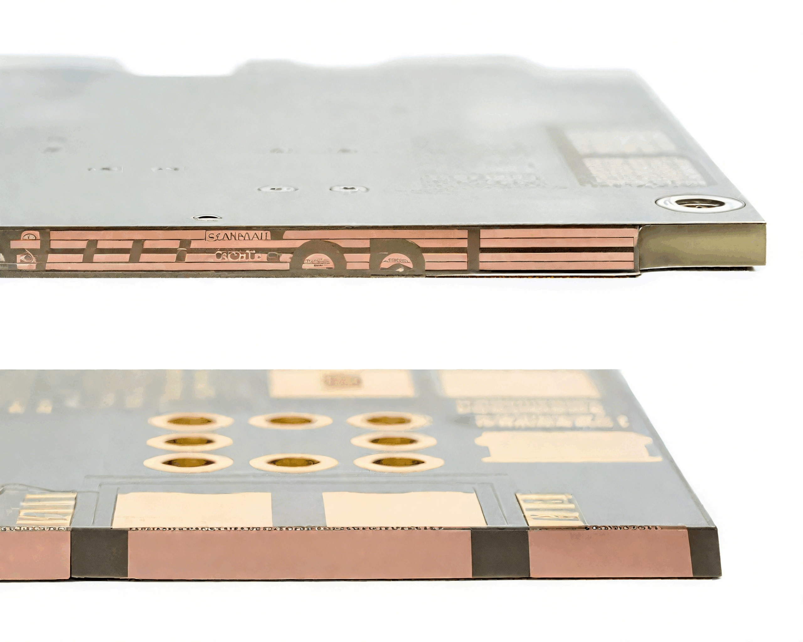
Multilayer adhesion is created in a few metres of process line. Before the layers are pressed together, the copper surfaces that will form the internal interfaces are cleaned, textured and oxidised so that the resin has something to grip and something to bond to chemically. If that treatment is inconsistent, the layers may still laminate and pass electrical test, and the weakness only appears later as delamination around a hole or as a blister after thermal cycling. This article explains what surface preparation has to achieve and how it is controlled.
What Adhesion Depends On
Two mechanisms hold an inner layer interface together. Mechanical interlocking depends on the surface area and the texture of the copper, which the treatment increases. Chemical bonding depends on the chemistry of the treated surface, which has to be compatible with the resin system being pressed against it.
Both mechanisms degrade if the surface is contaminated. Oil from handling, dust, residual resist, fingerprints and drying marks all reduce the effective contact between the resin and the copper. Because contamination is invisible after lamination, preparation and handling have to be controlled as a sequence rather than as a single step.
Mechanical Preparation
Mechanical preparation removes resist residue and creates a uniform surface for the chemical steps that follow. Brushing, pumice scrubbing and jet scrubbing are the common methods, and each leaves a characteristic texture. A brush that is worn or a pumice slurry that is overloaded produces an uneven surface, which shows up later as variation in adhesion across the panel.
The mechanical step also has a dimension effect. Aggressive scrubbing removes copper, and on a fine line pattern that reduction changes the conductor width and the impedance. The amount of copper removed should be monitored as a process parameter rather than left to the operator, because the effect is small per panel and large over a production run.
Chemical Preparation and Micro Etching
The chemical steps clean and activate the surface. A micro etch removes a controlled amount of copper, typically a fraction of a micrometre to a couple of micrometres, which exposes fresh metal and produces a uniformly textured surface. The etch rate depends on chemistry concentration, temperature and dwell time, so all three are controlled together.
Over etching and under etching both cause problems. Under etching leaves a surface that does not bond well, while over etching removes too much copper and can undercut fine features. The aim is a defined weight loss per panel, measured by a test coupon or by an in line monitor, rather than a visual judgement of how the surface looks.
Oxide Treatment and Its Types
The oxide layer is what the resin bonds to. It is grown chemically and its colour and morphology depend on the chemistry and the process conditions. The two families in common use differ in thickness and in structure, and the one chosen has to be compatible with the resin system and with the number of thermal cycles the product will see.
Oxide chemistry interacts with the laminate as much as with the process. Resins with a different chemistry may bond differently to the same oxide, and some high performance systems require a treatment that is adjusted for them. The material behaviour that determines this is described in PCB laminate material properties, and a change of material should trigger a review of the oxide process.
Drying and Handling After Treatment
A treated surface begins to degrade as soon as it is exposed to air. Moisture is absorbed, the oxide continues to grow or to change form, and contamination accumulates from the environment and from handling. The interval between treatment and lamination is therefore a controlled parameter, and it is usually specified as a maximum time rather than as a target.
Storage conditions matter during that interval. Dry, clean, temperature stable storage with interleaving that does not abrade the surface preserves the treatment, while open storage in a humid area does not. Gloves are required whenever a treated panel is handled, and panels should be handled by the edges so that the treated area is never touched.
Interaction With Lamination Parameters
Preparation and lamination are a single process in practice. The press profile has to bring the resin to a temperature and a viscosity that allows it to flow into the treated surface and then cure, and a surface that is prepared for one resin may not be ideal for another. Changing the press profile without reviewing the preparation is a common cause of adhesion problems that appear to be random.
The layer structure also matters. A stackup with many thin layers has more interfaces and therefore more opportunity for a weak bond, and the interfaces closest to the board edge see the most mechanical and thermal stress. The rules that determine a well balanced structure are described in multilayer layer assignment, and the interfaces that carry the most risk should be identified before the panel is processed.
Tests That Confirm the Bond
Adhesion is measured rather than assumed. Peel strength testing on a prepared sample and thermal stress testing by solder float or reflow are the standard screening methods, and both should be run whenever the preparation chemistry, the resin or the press profile changes. A sample that survives a solder float without blistering or delamination is the minimum evidence that the process is in control.
Production monitoring uses simpler checks: weight loss from the micro etch, oxide thickness or colour control, and a copper foil peel test on a panel from each lot. Where a failure does occur, the investigation should cover the preparation history and the press profile together, since the symptoms of a weak interface are the same from either cause. The inspection criteria used to judge the result are the same ones applied to other laminate quality questions, described in judging PCB quality.
Failure Modes and Their Signatures
Delamination around a plated hole after thermal cycling points to a weak interface combined with the stress of the barrel expansion. A blister between layers on a large copper area points to moisture trapped at the interface, which is usually a drying or storage problem. A halo of discolouration around a hole points to resin that was not fully cured or to contamination at that location.
A fourth signature is a pattern rather than a location: delamination that appears on one side of the panel and not the other usually points to an uneven treatment, such as a brush that is worn on one edge or a rinse that does not reach the whole surface. The gopcb fabrication group treats any of these as a process investigation rather than as a single panel defect. The preparation logs, the press records and the storage times are reviewed together, because the interface that failed was created by several steps and can only be corrected by finding which of them moved.
FAQ
How long can a treated panel wait before lamination? The supplier process specification defines the limit, and it is usually measured in hours rather than days. Once the limit is exceeded the treatment is normally repeated.
Does a thicker oxide always bond better? No. Oxide structure matters more than thickness, and an oxide that is too thick can be brittle and crack during lamination or thermal cycling.
Can adhesion problems be seen before thermal cycling? Sometimes, by a peel test or by inspection for haze, but often not. Thermal stress testing is the reliable screen.