OSP Surface Finish Process Control and Storage Guide
OSP, or organic solderability preservative, is a thin organic film that protects clean copper from oxidation without adding any metal to the surface. It is the cheapest of the common finishes, it is simple to apply, and it leaves the flattest possible surface for fine pitch printing. Its weakness is a limited thermal budget and a limited shelf life, so the process is really a story about control rather than about chemistry. For a product that is assembled soon after fabrication, an OSP finish is often the most cost effective choice available.
What OSP Is
The coating is formed by dipping the panel into a solution of an azole compound that reacts with the copper surface and grows a thin, tightly bonded film. The film is typically only a fraction of a micrometre thick, so the topography of the copper beneath it is essentially unchanged. In effect the protective film is a chemical rather than a metallurgical barrier, and it works only while it remains intact on the surface.
Because no metal is deposited, the finish adds nothing to the impedance of a trace and nothing to the thickness of a pad. That is why the process is often found on high frequency boards and on fine pitch assemblies, where a small change in surface geometry would matter. The absence of a metal layer also means no galvanic couple at the pad, so there is no risk of the corrosion mechanisms that affect some metallic finishes.
How the Coating Is Applied
Application is a short sequence: clean the copper, micro etch it, rinse it, apply the OSP in a controlled bath, rinse again and dry. The bath is normally slightly acidic and is operated at a moderate temperature, and the immersion time sets the film thickness. Every one of those stages is short, which makes the process productive and also leaves little room to recover from a mistake.
Contamination control matters more than the bath itself. Copper carried into the OSP tank from the etch line raises the metal content of the bath, and organic contamination from a poorly rinsed resist leaves a surface that will not form a coherent film. That film may still look clean while it repels the OSP chemistry, so a wetting check on the incoming panels is worth the few minutes it takes. Our solderability guide covers the tests used to confirm the result.

Thickness and Coverage
Film thickness is measured indirectly, because the layer is too thin for the usual X-ray methods. Weight difference on a coupon, a UV spectroscopic method or a simple colour and wetting check are all used, and the acceptance criterion is usually a minimum rather than a tight band.
Coverage is a more useful measure than thickness in most shops. A film that is present but discontinuous will protect most of the pad and fail at the edges, and the failure will appear as a dewetted area after reflow rather than as a coating defect before it. A board can therefore pass a visual inspection and still contain a pad that will not solder, which is the reason the wetting test exists.
Storage and Shelf Life
The film protects copper from the atmosphere but it is not permanent. It slowly loses its protective capability, and the rate depends on the temperature, the humidity and the airborne contamination of the store. A shelf life quoted in months assumes a defined storage condition. A shelf life quoted without a storage specification is meaningless, and the two should always be quoted and agreed together.
Packaging therefore does most of the work. A moisture barrier bag with a desiccant keeps the film intact for the full storage period, while an unprotected board in a humid room may lose solderability well before the nominal date. Our solderability guide explains how the surface condition is checked before assembly. A folded or punctured bag defeats the packaging completely, so the seal and the indicator card should be checked on receipt.
Solderability Through the Coating
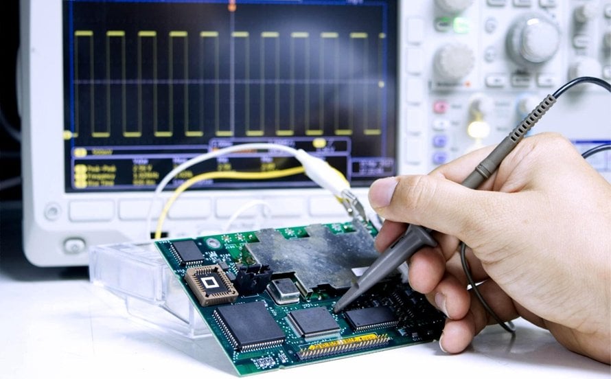
The coating dissolves in the flux during soldering and exposes fresh copper to the molten solder, so the flux has to be active enough to remove both the film and the oxide that has grown beneath it. A flux that works well on a metallic finish may be marginal on an OSP surface.
Where the coating is thick or has aged, the flux has less margin and the wetting becomes slower. That shows up as a longer wetting time rather than as a complete failure, which makes it easy to miss until a marginal process produces a run of cold or partial joints. Measuring the wetting time on a sample coupon before production starts is a cheap way to confirm that the flux has enough margin.
Multiple Reflow Exposures
Every reflow cycle consumes part of the coating, so a board that has to survive two or three passes is a different problem from one that sees a single pass. The first pass removes most of the film in the printed areas, and the second pass relies on whatever remains. Keeping the total thermal exposure to a minimum is the practical answer, and it may mean choosing a finish with a higher thermal budget for the second side.
A double sided assembly with a mixed technology step therefore needs a coating specified for the number of cycles it will see. Where the budget is tight, the process may need a different finish on the critical side. Our surface finish guide compares how the common finishes behave under multiple passes. The finish should be selected for the assembly flow, not for the first soldering operation alone.
Interaction with Plating and Mask
OSP is applied after the mask has been cured, because the high temperature of the mask cure would destroy the film. That ordering means the coating has to be applied to a board that already carries cured mask, and the mask must not bleed or release anything into the OSP bath.
Plated features such as a hard gold finger or a press fit hole are normally masked off during the OSP step, because the coating is not wanted on a noble metal surface. The masking material and its removal have to be compatible with the rest of the flow. Residue from a masking tape can leave a film that prevents the OSP from forming, and the tape removal step has to be verified.
Defects and Detection
The characteristic defect is a pad that will not wet, appearing as a dewetted area or a solder ball after reflow. It usually traces back to an incomplete film, a contaminated bath or a storage condition that exceeded the specification. Where the cause cannot be established, the lot should be treated as suspect and tested before it is released to assembly.
Because the film is invisible, detection depends on a wetting test or on process records rather than on inspection. A solderability test on a coupon from the lot, plus the storage record, is the evidence that the finish is still usable. Retaining a coupon from each lot and testing it at the end of the storage period is a simple and convincing control. Our quality documentation describes how these results are classified at gopcb.
Process Control Points
The controls are the copper surface preparation, the bath concentration and pH, the immersion time and temperature, the rinse quality and the drying, plus the packaging that follows. Every one of them is recorded per lot, and every one of them can drift during a long run. Bath life, immersion time and rinse quality are the three that change most often, and they should be checked at the start and the end of every shift.
The most useful single control is a wetting balance test on a coupon taken from each lot and repeated after the storage period. That test measures the property the customer cares about rather than the property the bath produces, and it converts a hidden risk into a number. That single measurement is worth more than a page of bath analysis data, because it measures the outcome rather than the input.
FAQ
Is OSP suitable for multiple reflow cycles? It can be, if the coating is specified for the number of cycles and the storage has been controlled. The first pass consumes most of the film, so the second pass has less margin.
Why does an OSP board fail to wet after storage? The film has aged or was never coherent, so the copper beneath it has oxidised. A solderability test on a coupon from the lot answers the question directly.
Can OSP be used on a board that will be wire bonded? No. The film has to be removed to expose bare copper, and even then the surface is not stable enough for reliable bonding. A metallic finish is required for that application.