Dead Copper in PCB Layout: Remove It or Keep It?
Dead copper is the copper left on a layer that no longer connects to any net. It appears wherever a pour is cut into isolated fragments by clearance, keepouts or traces, and it is usually removed automatically. The question worth asking is whether removal is always right, because in a small number of cases the fragment is doing something useful.
How Dead Copper Appears
When a copper pour is generated, the tool fills the empty space while keeping clearance from every trace, pad and hole. Small areas surrounded by clearance can end up enclosed, connected to nothing, and those enclosed areas are the islands that the removal setting targets.
They appear in predictable places: between the pins of a fine pitch device, inside a large via field, around connector footprints and anywhere a keepout has cut a pour into pieces. A dense board generates them in quantity, which is why most tools default to removing them.
Why Floating Copper Is a Problem
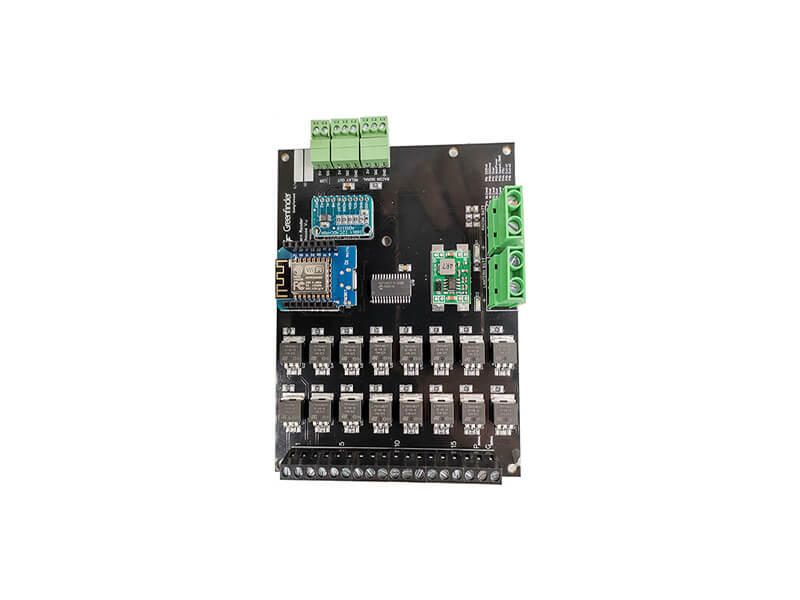
An island is a conductor at an undefined potential. It couples capacitively to whatever is nearby, so a fragment sitting under a fast clock net adds a small uncontrolled capacitance to that node and to the plane around it, and the effect changes with the layout.
It also behaves as a radiator. A floating patch can be excited by nearby fields and re-radiate, which is the opposite of the containment a ground plane is supposed to provide. On sensitive analogue circuits the coupling is small but unpredictable, and unpredictable is worse than absent.
<img src="https://www.gopcba.com/wp-content/uploads/2026/08/Array-of-Beryllium-Oxide-BeO-Ceramic-PCB-LED-boards-768×476-1.webp" alt="Copper pour with island removal enabled beside a ground plane” />
Manufacturing Reasons to Remove It
Fabrication gives an independent reason. Very small copper features can lift or detach during etching and plating, and a sliver that is not anchored to anything is the most likely feature on the panel to cause a problem. Removing them improves yield for the fabricator.
Inspection is affected as well. A dense field of small islands makes automatic optical inspection harder and produces false calls, which slows the line and increases the chance that a real defect is missed among the noise.
When a Fragment Is Worth Keeping
The exception is copper balance. On a thin core or a large panel, an uneven distribution of copper causes the board to warp during lamination and reflow, and a small island that is surrounded by empty space on one side may be helping to even it out.
Even then the fragment should be connected. Tying an island to the ground net with a via or a short trace removes the floating potential and keeps the balance, which gives both the electrical and the mechanical benefit at the cost of one via.
Tool Settings and Rule Configuration
Island removal is normally a property of the polygon rather than a global option, so it can be set per pour and treated as a design rule rather than a permanent tool preference. That granularity matters, because a pour on a digital layer and a pour on an analogue layer may need different treatment even on the same board.
The related settings are the minimum island area and the connection style. A threshold that removes everything below a small area is a reasonable default, while the copper flooding method, solid or hatched, determines how many fragments are produced in the first place.
Interaction With Plane Splits
Dead copper is most common where a plane has been divided. Splitting a plane into voltage regions creates slivers along the partition, and if the partition is drawn without regard to the pour, the fragments appear on both sides of it, as the rules for power plane partitioning describe.
The fix is to design the partition first and pour afterwards, keeping the boundaries simple and the clearances uniform. A partition that follows a straight line produces fewer islands than one that weaves between pads.
Thermal and Assembly Effects
An island can also affect soldering. A small disconnected area next to a pad changes the local heat capacity, which alters how quickly the joint reaches temperature, and on a wave or selective soldering process that difference can produce an inconsistent fillet.
Where copper is intended to spread heat, the connection has to be deliberate. A thermal pad that relies on the surrounding copper must be connected solidly or through a defined via array, and a floating fragment beside it contributes nothing to the thermal path.
Reviewing the Finished Pour
The pour should be reviewed after the layout is complete and again after any change to the outline, the stackup or the component placement. These edits move copper silently, and the regenerated pour may create or remove islands without any change to the routing.
A useful habit is to display the pour with the connectivity check enabled and look specifically for isolated regions. The check confirms that every area of copper belongs to a net, and where an island was deliberately retained, the connection to that net appears in the report rather than being assumed.
Dead Copper in Fine Pitch and HDI Areas
High density areas generate the most islands, because the clearance around each via and pad leaves very little room for a pour to fill. In a via field the remaining copper can be reduced to narrow webs that are connected, useful for thermal spreading and difficult to inspect.
The practical response is to accept the webs and remove the isolated slivers. Where the webs carry heat away from a power device, keeping them connected to the ground net is what turns a by-product of the pour into part of the thermal design.
Interaction With Stitching Vias
Stitching vias are often added to hold a pour at a defined potential and to tie reference planes together. Each via placed in a fragment converts that fragment from a floating conductor into part of the ground network, which is the cheapest possible way to keep copper that would otherwise be deleted.
Placement deserves some care. Vias sitting in isolation far from any trace provide almost no benefit, while a via in a fragment close to a signal trace anchors the local reference and can measurably improve the return path.
Checking Copper Density Before Release
Copper density per layer is a manufacturability parameter, not a cosmetic one. Uneven density causes different etch rates across the panel, changes the resin flow during lamination and affects how flat the finished board is, so most fabricators ask for it to be balanced.
A quick review of the density map shows whether one area of the board is starved while another is saturated. Adding connected copper in the sparse region, or using a hatched fill, restores the balance without the electrical penalty that a floating island carries.
Common Misunderstandings
One is that a pour improves a design simply by existing. Copper that is fragmented, floating or far from the signal it is supposed to reference contributes little and can make the return path harder to control than a plain area of bare laminate.
Another is that the removal setting is a global preference. It is applied per polygon, and a board that inherits a setting from another project may be pouring with a threshold that suits a different layer count and density, which is why the setting is worth confirming on every new layout.
FAQ
Should dead copper always be removed? In almost all cases yes, because a floating conductor couples and radiates unpredictably and gives the fabricator a feature that can detach during processing.
Does removing it change the impedance of nearby traces? Slightly, because the copper around a trace contributes to the local environment. Leaving the pour connected to ground rather than deleting it entirely keeps the environment closer to what was modelled.
Can an island cause a short? A floating fragment is not a short by itself, but if it bridges two nets after a manufacturing defect or deforms during assembly, it can create one. That risk is another reason it is normally removed.