Eight Layer Board: Impedance Control and Stackup Design
An eight layer board is the point at which a design stops being a set of stacked signal layers and starts being a controlled transmission environment. There are enough layers to give every high speed net a reference plane, enough planes to deliver power with low impedance, and enough freedom to route a dense device without compromising either. The cost of that freedom is that the decisions taken in the stackup are difficult to reverse later.
The two questions that shape the arrangement are where the reference planes go and which layers carry the fast nets. Everything else, including impedance control, signal integrity and the practical matter of keeping the board flat through assembly, follows from those two answers. It is worth settling them before a single trace is routed.
What Eight Layers Make Possible
A typical arrangement places a signal layer next to each plane, so that every fast net has a continuous reference within a few thousandths of an inch. That pairing is what makes impedance control practical: the trace geometry and the dielectric thickness between the trace and its plane are known, so the width follows from a calculation rather than from an experiment.
Eight layers also allow the power distribution to be separated from the signal returns. A dedicated power plane with a thin dielectric to the adjacent ground plane acts as a distributed capacitor across a useful band of frequencies, which reduces the number of decoupling parts required around a large device.
Choosing the Layer Assignment
The stackup design fixes the layer assignment before routing begins, and from that point the assignment is treated as a constraint. Signal layers adjacent to a plane are used for the fast nets, because their return current can flow directly underneath. The layer pair in the middle of the stack, which sits between two planes, is usually reserved for slower signals where a return path detour is tolerable.
Two signal layers placed next to each other without an intervening plane couple to one another rather than to a reference. That arrangement can still work, but the coupling has to be understood, and cross talk between the layers becomes a design parameter instead of an afterthought. It is a poor place for a clock or a sensitive analog net.

Impedance Control and Its Tolerances
Controlled impedance is a specification on the finished board, not on the drawing. The width that produces fifty ohms depends on the dielectric constant of the laminate, the thickness of the dielectric, the copper thickness after plating and the presence of solder mask over the trace, and each of those has a tolerance.
The practical consequence is that a supplier needs a tolerance window rather than a single number. Where a net is sensitive, the specification should state the target and the acceptable band, and the supplier’s test coupon is the evidence that the band was held. A coupon measured on one panel speaks for the process, not for every trace on every board.
Reference Plane Integrity
A plane is only a reference where it is continuous. A cut in the plane, whether from a connector footprint, a via field or a deliberately isolated region, forces the return current to divert around it, and the resulting loop behaves like an inductor in series with the return path of every net that crosses the gap.
Where a plane has to be divided, the division should be made along a line that no fast net crosses, and the two regions should be joined at a defined point. Stitching vias placed along the boundary keep the two planes at the same potential at high frequency, which is what makes the arrangement behave like a single reference rather than two.
Signal Integrity at the Layer Transition
A net that changes layers has to change reference planes as well, and the return current has to follow. The standard solution is a ground via close to the signal via, which gives the return a short path between the planes. Without it, the return current finds its own way through the plane capacitance, and the resulting discontinuity shows up as ringing on a fast edge.
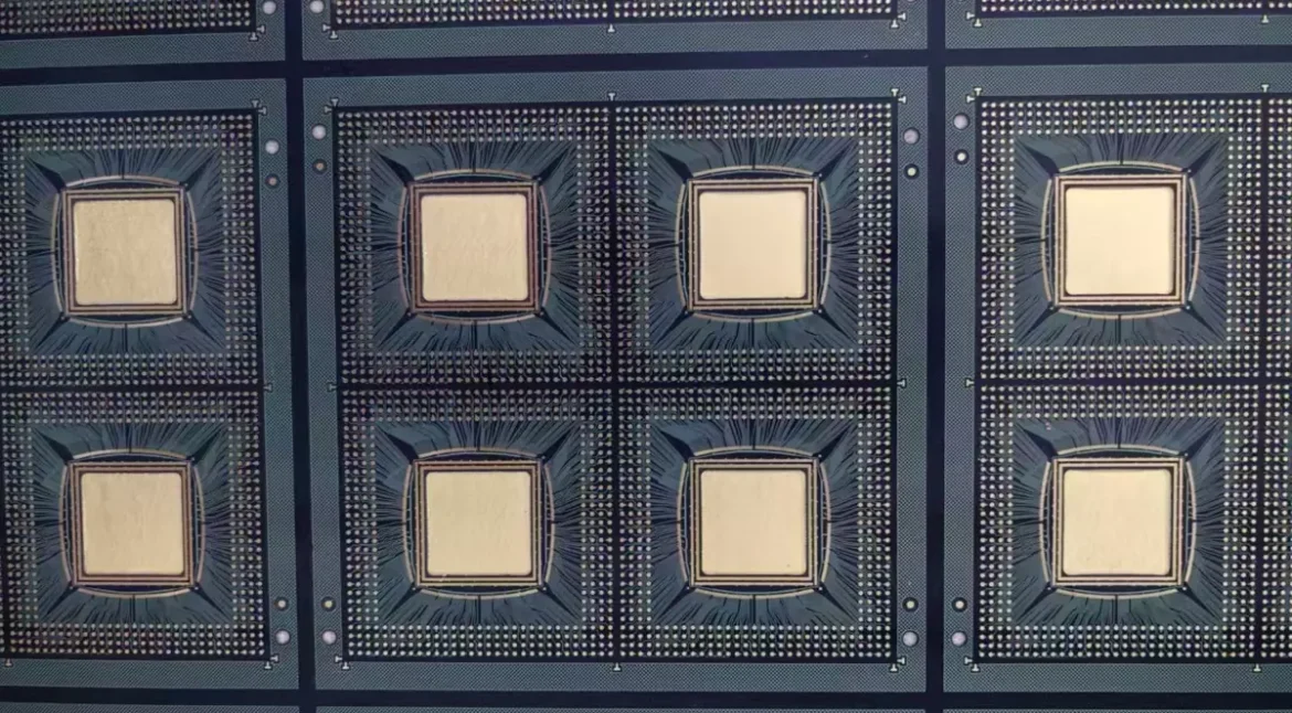
Where a connector or a package forces a group of signals to change layers together, the same treatment applies to the whole group. The stitched region under a ball grid array is a good example of the practice, and the reasoning behind it is set out in the discussion of impedance discontinuity.
Power Distribution on the Plane Pair
Once the power and ground planes are adjacent, the impedance between them at high frequency is set by the plane geometry rather than by the capacitors. The capacitors handle the lower frequencies where their own inductance is small, and the plane pair takes over above the point where the capacitor loop becomes inductive.
The design work is therefore to keep the plane pair intact under the devices that draw the fast current, and to place the capacitors where their loops are short. A device surrounded by a plane pair with a low impedance is much easier to decouple than one that relies on a network of parts connected through vias.

Thickness, Bow and Assembly
An eight layer board is thick enough that the balance of the construction matters. Symmetry in the sequence of cores and prepregs, and reasonable balance in the copper distribution between layers, keep the panel flat through the lamination and through the reflow cycles that follow.
Thickness also affects the drilling and the via behaviour. A taller board means a longer barrel for any given drill, a higher aspect ratio for the plating process and a longer stub for a through via. Where the stack has to be thick for mechanical reasons, back drilling becomes a way to keep the electrical performance of the fast nets, and the board thickness guide sets out the practical range.
When a Simpler Board Would Do
Not every design that could use eight layers should. A board with a single fast interface and a modest pin count can often be built on six or even four layers with a careful assignment, and the saving is real. The technique earns its place where several dense devices, a parallel bus or a tight impedance requirement are present.
The honest test is whether the extra layers are doing work. If two of them exist only to provide a return path that a better placement would have made unnecessary, the design is paying for a stackup instead of solving a layout problem. That distinction is one of the themes of the broader guidance on multilayer boards for high speed designs.
FAQ
Is eight layers enough for a fast memory interface? Usually, provided the bus has a continuous reference on every layer it uses and the skew budget is respected. The limit is the routing channels around the device rather than the layer count itself.
Does a thicker dielectric hurt impedance control? It widens the trace needed for a given impedance, which costs routing space. It also raises the via stub resonance, so the trade has to be considered together.
How is the finished impedance confirmed? With a test coupon on the production panel, measured against the target and the tolerance band. Coupons are built with the same process as the boards and travel with them through fabrication.