Electronic assembly is one of the most important stages in modern electronics manufacturing. It transforms a bare printed circuit board (PCB) into a functional electronic assembly by accurately mounting and soldering components such as resistors, capacitors, diodes, integrated circuits, connectors, sensors, and power devices.
From smartphones and consumer electronics to industrial automation, automotive electronics, medical equipment, telecommunications, and aerospace systems, the quality of PCB electronic assembly has a direct impact on electrical performance, reliability, manufacturability, and product life.
As electronic products become smaller while delivering higher processing power and greater functionality, manufacturers face increasing demands for high-density PCB assembly, fine-pitch components, high-speed signal transmission, thermal management, miniaturization, and reliable production at different volume levels.
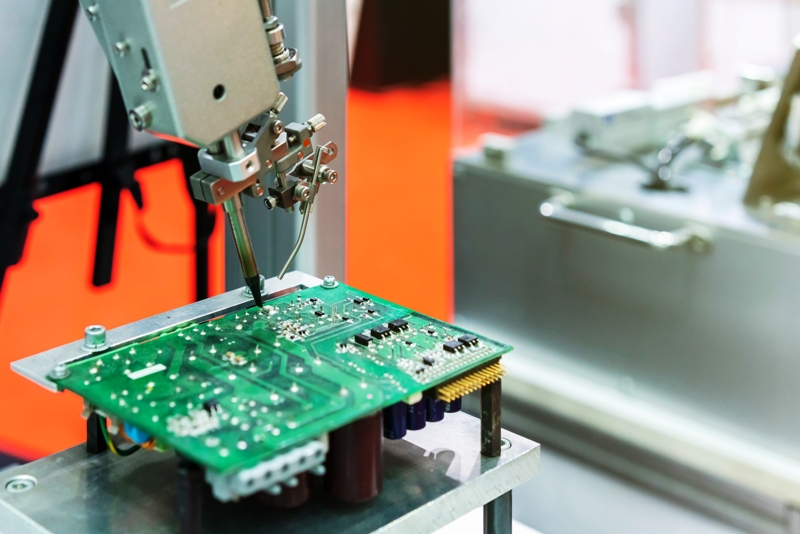
Modern electronic assembly is therefore much more than simply attaching components to a circuit board. It combines engineering analysis, component procurement, SMT and THT assembly, soldering, automated inspection, electrical testing, traceability, and quality management into a controlled manufacturing process.
This guide explains what electronic assembly is, the main PCB assembly technologies, the complete assembly process, common applications, design considerations, inspection methods, and how to select a reliable electronic assembly manufacturer.
What Is Electronic Assembly?
Electronic assembly is the process of mounting, soldering, inspecting, and testing electronic components on a PCB to create a functional PCBA (Printed Circuit Board Assembly).
A bare PCB provides conductive traces, pads, vias, reference planes, and mechanical support, but it does not perform the intended electronic functions until the required components are installed.
A typical PCB assembly process includes:
Engineering Review → BOM Verification → PCB Fabrication → Component Sourcing → Solder Paste Printing → Component Placement → Reflow Soldering → THT Assembly → Inspection → Electrical Testing → Functional Testing → Packaging
Depending on the product, additional processes may include conformal coating, potting, heat-sink installation, IC programming, cable assembly, labeling, and box-build integration.
The objective is to create an assembly in which every component is correctly positioned, securely soldered, electrically connected, and able to perform according to the original product specification.
PCB Fabrication vs. Electronic Assembly
PCB fabrication and electronic assembly are two closely related but different stages of electronics manufacturing.
| Feature | PCB Fabrication | Electronic Assembly |
|---|---|---|
| Definition | Manufacturing the bare circuit board | Populating and soldering components onto the PCB |
| Main Materials | Laminate, copper foil, prepreg, solder mask | ICs, resistors, capacitors, connectors, sensors, etc. |
| Main Processes | Imaging, etching, lamination, drilling, plating, finishing | Printing, placement, soldering, inspection, testing |
| Output | Bare PCB | Functional PCBA |
| Components | No components installed | Electronic components installed |
| Main Quality Focus | Layer registration, copper, drilling, impedance, surface finish | Placement accuracy, solder quality, component quality, functionality |
A reliable manufacturing workflow must consider both stages together. A PCB that is correctly fabricated may still encounter assembly problems if the component footprints, pad dimensions, spacing, thermal design, or manufacturing data are incorrect.
This is why DFM (Design for Manufacturability) and DFA (Design for Assembly) are essential parts of the engineering process before production.
Main Types of Electronic Assembly
The electronics industry primarily uses SMT assembly, THT assembly, and a combination of both technologies.
Surface-Mount Technology (SMT)
Surface-Mount Technology (SMT) mounts electronic components directly onto solder pads on the surface of a PCB.
Unlike through-hole components, SMT components generally do not require leads to pass through the entire PCB. This enables smaller component packages and significantly higher circuit density.
Typical SMT components include:
- Resistors
- Capacitors
- Diodes
- Transistors
- MOSFETs
- QFN
- QFP
- BGA
- LGA
- CSP
- Microcontrollers
- Memory devices
- Power-management ICs
Advantages of SMT PCB Assembly
Miniaturization: Small SMT packages allow manufacturers to create compact electronic products.
High Component Density: Components can be mounted on both sides of the PCB.
Automation: High-speed pick-and-place machines can install large numbers of components with repeatable precision.
Manufacturing Efficiency: Automated solder paste printing, placement, and reflow can support high-volume production.
High-Speed Compatibility: Shorter electrical interconnects can help reduce parasitic effects in high-speed circuit designs.
Through-Hole Technology (THT)
Through-Hole Technology (THT) inserts component leads through drilled holes in the PCB before soldering.
THT is still widely used for components requiring additional mechanical strength or larger electrical connections.
Typical applications include:
- Connectors
- Transformers
- Relays
- Large capacitors
- Terminal blocks
- Power components
- Switches
Advantages of THT Assembly
High Mechanical Strength: Component leads pass through the PCB, creating robust mechanical connections.
Vibration Resistance: THT is particularly useful for industrial and automotive products exposed to mechanical stress.
High Power Handling: Larger through-hole components can accommodate high-current and high-power applications.
Serviceability: Some THT components are easier to inspect, manually solder, and replace during repair.
Mixed-Technology PCB Assembly
Modern products frequently combine SMT and THT assembly.
For example, a control board may use miniature SMT components for processors, memory, resistors, and capacitors while using THT connectors, relays, transformers, or power components.
This approach is known as mixed-technology PCB assembly.
A properly optimized mixed-technology process combines the density and efficiency of SMT with the mechanical strength and power-handling capability of THT.
Electronic Assembly Process: Step by Step
1. Engineering and Design Review
Before production begins, the manufacturer reviews the customer’s manufacturing package.
A typical package contains:
- Gerber files
- BOM
- Pick-and-place files
- Assembly drawings
- Schematic
- PCB stackup
- Component specifications
- Testing requirements
The engineering team checks whether the information is consistent and suitable for manufacturing.
Typical checks include:
BOM Verification: Confirming manufacturer part numbers, quantities, package types, and approved alternatives.
Footprint Verification: Ensuring component footprints match physical component packages.
Placement Verification: Confirming component coordinates and rotations.
Assembly Feasibility: Checking spacing, pad geometry, polarity markings, component height, and accessibility.
DFM/DFA Analysis: Identifying potential manufacturing and assembly risks before production.
Early engineering review can prevent expensive production interruptions and reduce unnecessary prototype iterations.
2. Solder Paste Printing
For SMT assembly, solder paste printing is usually the first physical assembly operation.
A stainless-steel stencil is aligned with the PCB. A controlled squeegee motion then deposits solder paste through stencil apertures onto the required PCB pads.
Printing accuracy directly affects solder-joint quality.
Important factors include:
- Stencil thickness
- Aperture dimensions
- Solder paste type
- Squeegee pressure
- Printing speed
- Board support
- Stencil alignment
Modern production lines can use SPI (Solder Paste Inspection) to automatically measure solder-paste volume, height, area, and position.
This provides an early opportunity to detect printing problems before components are placed.
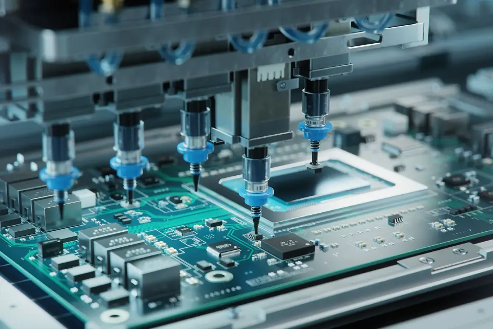
3. SMT Component Placement
After solder paste printing, pick-and-place machines install SMT components.
High-speed placement equipment uses vision systems to identify PCB fiducials and confirm component position and orientation.
The process must accurately control:
- X/Y coordinates
- Rotation
- Component polarity
- Feeder position
- Placement force
- Component orientation
Modern SMT equipment can support miniature components and fine-pitch semiconductor packages while maintaining highly repeatable placement accuracy.
4. Reflow Soldering
Following placement, the PCB passes through a controlled reflow soldering oven.
The board is gradually heated through several thermal zones:
Preheat → Soak → Reflow → Cooling
During the reflow phase, the solder paste melts and forms permanent electrical and mechanical connections.
The thermal profile must be optimized according to:
- Solder alloy
- Component specifications
- PCB thickness
- Copper distribution
- Component density
- PCB material
Poor reflow control can cause:
- Cold solder joints
- Insufficient wetting
- Solder bridges
- Tombstoning
- Component damage
- Warpage
- Delamination
For high-reliability applications, reflow profiling and thermal process control are especially important.
5. THT Component Assembly
After SMT assembly, THT components can be installed where required.
Depending on the design and production volume, the manufacturer may use:
- Manual insertion
- Automated insertion
- Wave soldering
- Selective soldering
- Manual soldering
Wave soldering is suitable for many through-hole joints in larger production runs.
Selective soldering is useful for mixed-technology boards because it allows specific solder joints to be processed while minimizing thermal exposure to surrounding SMT components.
Kingda’s published THT capabilities include manual and automated insertion, lead-free/RoHS soldering, wave soldering, selective soldering, conformal coating, IC programming, inspection, and functional testing.
Inspection and Testing in Electronic Assembly
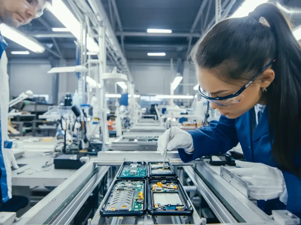
A professional PCB assembly manufacturer should use multiple inspection and testing methods because no single technique can detect every possible defect.
SPI — Solder Paste Inspection
SPI checks solder paste before component placement.
It can identify:
- Insufficient paste
- Excessive paste
- Misalignment
- Bridging risk
- Printing variation
Detecting problems at this stage can prevent them from becoming solder-joint defects after reflow.
AOI — Automated Optical Inspection
AOI uses cameras and software to inspect assembled PCBs.
It can identify:
- Missing components
- Incorrect placement
- Incorrect polarity
- Component displacement
- Tombstoning
- Solder bridges
- Visible solder defects
AOI is particularly valuable for high-volume and high-density SMT assembly.
X-Ray Inspection
X-ray PCB inspection is used for solder joints that cannot be directly observed from the surface.
It is especially useful for:
- BGA
- QFN
- LGA
- CSP
- Bottom-terminated components
X-ray can reveal:
- Voids
- Insufficient solder
- Hidden bridging
- Open joints
- Internal alignment problems
ICT — In-Circuit Testing
In-Circuit Testing (ICT) uses dedicated test fixtures and test points to evaluate electrical characteristics.
Depending on the test coverage, ICT can identify:
- Open circuits
- Shorts
- Incorrect components
- Component-value errors
- Polarity errors
- Certain soldering defects
Functional Testing
Functional testing (FCT) evaluates whether the completed PCBA performs according to its intended application.
Tests may include:
- Voltage and current
- Digital interfaces
- Communication ports
- Sensors
- Displays
- Motors
- Relays
- RF functions
- Firmware
- Network communication
For complex systems, functional testing is often an important final validation step before shipment.
Best Practices for Electronic Assembly
Optimize Component Placement
Component placement should consider electrical, thermal, mechanical, and manufacturing requirements simultaneously.
High-speed components should be placed to minimize unnecessary trace length.
Heat-generating components should be positioned near appropriate thermal paths.
Polarized components such as diodes, LEDs, and electrolytic capacitors should have clear polarity indicators.
Keep Decoupling Capacitors Close to Power Pins
Decoupling capacitors should generally be placed close to IC power pins.
Short connections help reduce parasitic inductance and improve local power integrity.
This is particularly important in high-speed digital and mixed-signal circuits.
Plan Thermal Management During PCB Design
Thermal management should be considered before assembly rather than after thermal problems appear.
Possible solutions include:
- Thermal vias
- Copper planes
- Copper pours
- Heat sinks
- Metal-core PCB construction
- Thermal interface materials
- High-Tg laminate
The correct solution depends on the power density and environmental conditions of the product.
Apply DFM and DFA Principles
DFM evaluates whether the board can be fabricated efficiently.
DFA evaluates whether components can be assembled efficiently and consistently.
A professional review may identify:
- Insufficient component clearance
- Incorrect footprints
- Difficult-to-solder areas
- Poor test-point accessibility
- Component conflicts
- Panelization problems
- Manufacturing risks
Applying DFM/DFA before production can reduce defects and improve first-pass yield.
Consider Component Lifecycle and Availability
A component should not be selected only because it satisfies the electrical specification.
Engineers should also consider:
- Manufacturer
- MPN
- Lifecycle status
- Availability
- Lead time
- Approved alternatives
- Supply-chain stability
- Regulatory compliance
This is especially important for automotive, medical, industrial, and other long-lifecycle products.
Applications of Electronic Assembly
Consumer Electronics
Electronic assembly is essential for:
- Smartphones
- Tablets
- Laptops
- Wearables
- Smart-home products
- Gaming devices
The use of SMT enables compact products with high levels of functionality.
Automotive Electronics
Modern vehicles contain extensive PCB assemblies in:
- Engine control systems
- Battery management systems
- ADAS
- Infotainment
- Instrument clusters
- Lighting systems
- Body control modules
Automotive PCB assembly requires strong process consistency and environmental reliability.
Industrial Automation
Industrial electronic assemblies are used in:
- PLCs
- Motor controllers
- Industrial sensors
- HMIs
- Robotics
- Motion-control systems
- Industrial networking equipment
These products frequently operate continuously in environments involving vibration, dust, temperature variation, and electrical noise.
Medical Electronics
Medical equipment uses PCB assemblies in:
- Patient monitoring
- Diagnostic equipment
- Medical imaging
- Laboratory instruments
- Portable medical devices
- Therapeutic equipment
Medical electronics require careful quality control, traceability, documentation, and process consistency.
Telecommunications
High-performance PCB assemblies support:
- Routers
- Network switches
- Wireless communication equipment
- RF systems
- Data-center equipment
These applications often require controlled impedance, high-density routing, advanced materials, and precise assembly.
How to Select a Reliable Electronic Assembly Manufacturer
Choosing an electronic assembly manufacturer should involve more than comparing unit prices.
Engineering Capabilities
Look for a supplier that can provide:
- DFM review
- DFA analysis
- DFT support
- BOM verification
- Component lifecycle analysis
- Assembly process optimization
- Engineering troubleshooting
Manufacturing Capabilities
Confirm that the supplier supports the required:
- SMT
- THT
- Mixed-technology assembly
- BGA
- QFN
- Fine-pitch components
- Prototype production
- Low-volume production
- High-volume manufacturing
Quality and Inspection
A capable manufacturer should have access to:
- SPI
- AOI
- X-ray
- ICT
- FCT
- FAI
- Electrical testing
- Traceability systems
The exact combination should be defined based on product complexity and reliability requirements.
Why Choose Kingda for Electronic Assembly?
Kingda is a one-stop electronics manufacturing provider founded in 2013, integrating PCB design and development, PCB manufacturing, component procurement, SMT, DIP, finished-product assembly, and testing. The company serves customers across medical, automotive, industrial automation, AI, smart-home, security, power, and communication applications.
One-Stop PCB and PCBA Manufacturing
Kingda integrates:
PCB Design → PCB Fabrication → Component Procurement → SMT/THT Assembly → Inspection → Testing → Finished Product Integration
This reduces the number of supplier handoffs and simplifies project management.
Advanced SMT Assembly Capability
Kingda’s published PCBA capabilities cover a broad range of component packages, including 01005, 0201, BGA, LGA, PQFN, and fine-pitch devices. Its manufacturing capabilities include automated SMT assembly and inspection technologies such as SPI, AOI, and X-ray.
Prototype to High-Volume Production
Kingda supports prototype PCB assembly, low-volume production, medium-volume manufacturing, and high-volume PCB assembly, allowing customers to continue working with the same manufacturing partner as demand grows.
Strong Engineering Support
Kingda provides engineering support including DFM, DFA, DFX, manufacturing optimization, PCB design review, BOM analysis, and process improvement.
This engineering involvement helps identify manufacturing risks before they become production problems.
Stable Component Supply Chain
Kingda incorporates component sourcing and supply-chain management into its one-stop PCBA services. The company states that it maintains stable supplier relationships to support material availability and delivery requirements.
Comprehensive Quality Control
Kingda’s published quality system includes IQC, IPQC, OQA, AOI, X-ray, electrical testing, functional testing, and process monitoring. The company also states that its manufacturing systems provide product-process traceability.
International Certifications
Kingda states that it holds ISO 9001:2015, ISO 13485:2016, IATF 16949:2016, ISO 14001:2015, and UL certification, and is an IPC member.
These certifications are particularly relevant to customers operating in medical, automotive, industrial, and other quality-sensitive markets.
Electronic Assembly Checklist
Before sending a project to an electronic assembly manufacturer, engineers should confirm:
Design
- Schematic finalized
- PCB layout verified
- DFM/DFA completed
- PCB stackup confirmed
- Component footprints checked
- Thermal requirements defined
Manufacturing Data
- Gerber or ODB++ files
- NC drill files
- Complete BOM
- Manufacturer Part Numbers
- Pick-and-place file
- Assembly drawing
- Special process instructions
Components
- Availability confirmed
- Lifecycle status checked
- Approved alternatives identified
- Counterfeit prevention requirements defined
- Regulatory requirements reviewed
Assembly
- SMT/THT requirements defined
- Solder alloy specified
- Reflow profile requirements confirmed
- Cleaning requirements defined
- Conformal coating requirements identified
Testing
- SPI requirements
- AOI requirements
- X-ray requirements
- ICT/FCT requirements
- Functional test procedures
- Traceability requirements
- Final inspection criteria
Conclusion
Electronic assembly is the manufacturing stage that transforms a bare PCB into a functional electronic product. It combines component sourcing, placement, soldering, inspection, testing, and quality management to deliver a reliable PCBA.
The three major approaches—SMT assembly, THT assembly, and mixed-technology PCB assembly—allow manufacturers to select the most appropriate production strategy according to component type, electrical requirements, mechanical strength, thermal performance, product complexity, and production volume.
However, successful PCB assembly starts long before components reach the production line. Accurate engineering data, reliable components, DFM/DFA analysis, optimized placement, controlled soldering, comprehensive inspection, and functional testing all contribute to final product quality.
For companies developing complex electronic products, an experienced PCB assembly manufacturer can provide significant value by integrating engineering, procurement, manufacturing, testing, and quality control into one coordinated workflow.
Kingda provides a one-stop PCB and PCBA manufacturing solution covering PCB fabrication, component sourcing, SMT/THT assembly, inspection, testing, and finished-product integration. With support for prototype, low-volume, and high-volume production, combined with engineering services and internationally recognized quality certifications, Kingda can support electronics companies through the complete development cycle from prototype to production.