
Electronic PCB Assembly: Design Rules That Improve Assembly Yield
Assembly is the last chance to influence yield, and by the time a bare board reaches the placement machine most of the cost has already been committed. The design decisions that determine whether the assembly runs smoothly are made months earlier: which side the components sit on, whether the parts can be placed by machine, whether the joints can be inspected, and whether the panel can be handled. Good electronic PCB assembly outcomes come from designing for the process rather than from optimizing the process around the design.
The requirements differ by product. A high-reliability assembly in a critical system carries stricter acceptance criteria and more documentation than a consumer product, and the design should reflect the class it will be built to rather than a single generic standard.
Define the Constraints Before the Layout
Several constraints shape the assembly and should be identified at the start. Delivery requirements determine how much schedule risk the program can absorb. The operating life of the product determines how much thermal and mechanical margin the joints need. Component restrictions, including the need for traceable sourcing and protection against counterfeit parts, may exclude otherwise suitable devices. The acceptance quality limit and the inspection class determine how much inspection is required and what defect rate is acceptable. Yield targets determine how much process margin the design should carry.
Where these constraints are not written down, the design defaults to a general-purpose assembly and the mismatch becomes visible only when the first build fails an inspection criterion that no one had specified.
Test requirements belong in the same list. The only way to know whether an assembly meets its intent is to test it, and whether that test is a functional check, an in-circuit measurement, or a boundary-scan sequence changes the access that must be designed into the board.
Source Components for Manufacturability
Component selection is an assembly decision as much as an electrical one. Parts should come from sources that can supply the production volume with a documented chain of custody, and where a component is single sourced, the risk of a shortage during the build should be quantified rather than assumed away.
Availability also affects the package choice. A device available in two package options is an advantage when one of them is difficult to place or inspect, and a part that is only available in a package the assembly house cannot handle reliably is a problem that surfaces at the worst possible time.
Keep the Design Package Complete
The assembly house can only build what it is given. A complete package includes the material specification, the layout, the stackup, the bill of materials with manufacturer part numbers and approved alternates, the assembly drawing with polarity and orientation, and any special instructions such as coatings, torque values, or handling restrictions.
Ambiguity in this package is the most common cause of a delayed or incorrect build, because the assembly house has to stop and ask. Where a requirement cannot be drawn, it should be written, and where it can be drawn, it should not be left to a note.
Match the BOM to the Layout
The bill of materials and the layout must agree on every component. A mismatch between the footprint in the layout and the package specified in the BOM produces either a part that does not fit or a placement program that looks for a component that does not exist. Both are caught only by a deliberate cross-check, which is cheap compared to the cost of a build interruption.
The cross-check should be performed after the last layout change and before the files are released, and it should cover reference designators, values, tolerances, and package names. A tolerance difference that is invisible in the schematic can be a functional defect in the assembled product.
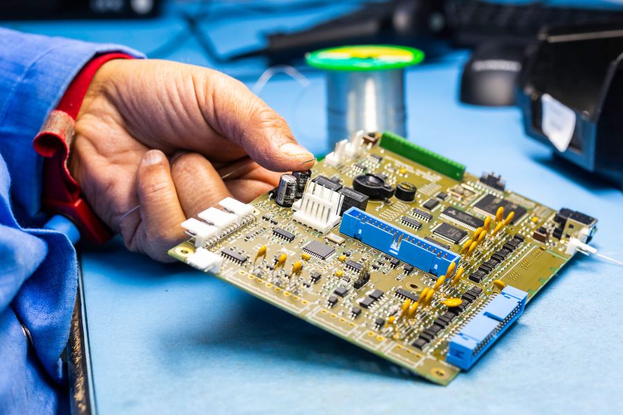
<img src="https://www.gopcba.com/wp-content/uploads/2026/09/266-1.jpg" alt="Design for assembly review of component placement on a PCB” />
Where the design uses approved alternates, the alternate should have the same footprint as the primary part. An alternate that changes the package is a design change, not a substitution.
Prefer Surface Mount and Single-Side Placement
Design for assembly begins with minimizing the number of distinct processes. Surface-mount parts are placed and soldered in one pass, while through-hole parts require insertion and a separate soldering step, and mixing the two in quantity lengthens the build and adds a thermal cycle. Replacing a through-hole part with a surface-mount equivalent, where the electrical and thermal requirements allow, removes a process from the flow.
Single-sided placement follows the same logic. Placing all components on one side means the board passes through the line once, with no inversion, no adhesive, and no second reflow. The cost is board area, which is often a reasonable trade against the process savings and the reduced risk to the parts. Where both sides must be used, the heavy and thermally sensitive parts belong on the side that is reflowed once.
Apply Design for Assembly Rules
The remaining rules are about access and predictability. Keep the component spacing consistent with the process capability described in placement order and pad positioning. Orient polarized parts consistently so that an operator or a vision system can verify them at a glance. Provide fiducials for the placement machine, and keep them clear of the panel edge and of any area that will be covered by a fixture.
Silkscreen should help rather than hinder: reference designators must not sit under components, and polarity markings must remain visible after assembly. Where a part is likely to be replaced, provide enough clearance for a rework tool, because a part that cannot be removed without damaging a neighbor will be removed anyway, and the board will suffer for it.
Pad geometry deserves its own review, since an undersized or oversized land is a direct cause of defects such as tombstoning and insufficient fillets. The standards are described in PCB pad design standards, and the mechanisms behind placement defects are covered in SMT component shift causes.
Plan Inspection and Incoming Verification
Inspection access is designed, not added. Automated optical inspection needs line of sight to the joints, which means tall components should not shadow their neighbors and connectors should not sit where they block a camera angle. X-ray inspection covers the joints that cannot be seen, including those under area-array packages and in through-hole barrels.
Incoming inspection closes the remaining gap by verifying the parts rather than the assembly. A counterfeit or out-of-specification component that reaches the placement machine can fail in a way that no assembly process control will catch, and the resulting investigation will consume far more time than the incoming test would have.
FAQ
Does a design for assembly review delay the project? It usually shortens it. The review takes a few hours and typically prevents a build interruption or a rework cycle, both of which cost days. The review is most valuable before the layout is released, when changes are still free.
Why does mixing through-hole and surface-mount parts increase cost? Because it adds a process step and a thermal cycle. The assembly must be reflowed for the surface-mount content and then wave or selectively soldered for the through-hole content, which requires additional tooling and exposes the parts to more heat.
How complete should the assembly drawing be? Complete enough that the assembly house does not need to ask a question. That means component positions, polarity, reference designators, the side each part is placed on, and any special process requirement. A drawing that requires interpretation will be interpreted differently by different operators.