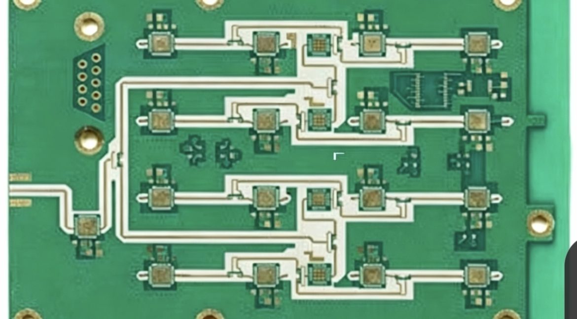
Etch Compensation: Holding Line Width Through the Etcher
Etch compensation is the correction applied to artwork so that the conductor that comes out of the etcher matches the width the designer asked for. The etchant removes copper sideways as well as downwards, so a trace drawn at a nominal width always finishes narrower, and the amount it loses depends on the copper thickness, the chemistry and the conveyor speed.
What Etching Actually Removes
The resist pattern defines where copper is protected, and the etchant attacks everything else. Because the attack is chemical rather than directional, it continues under the edge of the resist for as long as the panel is in contact with the chemistry, which produces the characteristic trapezoidal cross section of an etched trace.
The top of the trace is narrower than the bottom, and the sides are sloped rather than vertical. A designer who assumes a rectangular cross section will therefore overestimate the copper area, and the error grows as the trace gets finer relative to the copper thickness. A drawing that specifies a width without a tolerance is therefore only half a specification.
The Etch Factor Explained
The etch factor is the ratio of the depth etched to the sideways undercut, and it is the single number that summarises how a process behaves. A high etch factor means the chemistry cuts downwards much faster than sideways, which produces a nearly vertical wall and a trace close to the drawn width.
Etch factor falls as copper thickness rises, because the etchant has to work for longer to clear a thicker layer and the sideways attack continues for the whole of that time. That is why heavy copper boards need compensation values that would be unthinkable on a half ounce layer, and why fine line work is almost always built on thin copper instead. Our etching process notes describe the line in more detail.

Why Copper Thickness Changes Everything
Copper thickness is the dominant variable in the compensation calculation. A one ounce layer might lose fifteen microns from each side during a normal etch, while a three ounce layer of the same artwork loses considerably more before the last of the copper between the traces clears.
Thickness also varies across the panel, because plating is never perfectly uniform and a heavy copper board is usually pattern plated rather than panel plated. Where the copper is thicker in the middle of the panel than at the edges, one compensation value cannot be correct everywhere. Uniformity is a plating question before it ever becomes an etch question.
Artwork Scaling and Compensation Tables
Shops handle this with compensation tables that relate the target width, the copper weight and the process to a correction applied when the artwork is generated. The table is developed by etching test patterns and measuring the result, not by calculation alone, because every line behaves differently.
Artwork scaling is applied at the same time, since the laminate also shrinks during lamination and the image has to be enlarged slightly to compensate. The two corrections are independent, and one is a dimensional change of the whole image while the other is a change to every feature individually. Confusing the two produces a panel that is dimensionally correct and electrically wrong.

Compensation for Inner and Outer Layers
Inner layers are etched after imaging and before lamination, so the compensation has to account for the pressing step that follows. Outer layers are etched after the plating operation, so the copper thickness they carry is the base foil plus the plated deposit, which is larger than the designer’s nominal figure.
That difference is why the same nominal trace width produces a different finished width on an inner and an outer layer of the same design. Where a differential pair runs from an inner layer to an outer layer, the impedance changes with it, and the field solver should use the finished dimensions rather than the drawn ones. A design that crosses layers should be verified on both, because the etch histories are different.
Impedance, Resistance and the Consequences
At high frequency a ten percent error in line width moves the impedance by roughly five percent, which is enough to spoil a return loss budget on a controlled impedance design. On a power trace the same error changes the resistance and therefore the voltage drop and the heating. The two requirements rarely agree on which direction of error is the more dangerous.
The errors do not have to be large to matter. A trace that finishes at ninety percent of its drawn width carries about ten percent less current for the same temperature rise, and the cumulative effect across a dense board is a design that works on the bench and fails in the field. A nominal width on a drawing is a starting point rather than a guarantee.
Measuring and Verifying the Result
The measurement is made on a coupon rather than on the product, using an optical system that reads the top and bottom widths of the trace at several points. The result is compared with the target, and the difference is what feeds back into the compensation table.
Consistency matters more than the absolute value. A panel that is uniformly half a micron narrow can be compensated, while a panel that varies across its area cannot, and the variation is usually the symptom of a plating or conveyor problem rather than an etch one. A test coupon that travels with the panel is what makes that comparison possible.
Process Control on the Etch Line
Etch rate changes with chemistry concentration, temperature, spray pressure and conveyor speed, so all four are controlled and recorded. A change in any one of them shifts the finished width, and a line that is adjusted without recording it loses the link between the compensation table and the panels it produced. Chemistry analysis, temperature logs and conveyor speed are all part of the same record.
Loading also matters, because a heavily loaded panel consumes more of the etchant locally than a lightly loaded one. That is why copper balance across the panel influences the result, and our copper balance notes explain how thieving is used to even it out. Pattern density changes the local etch rate as well, so a sparse area behaves differently from a dense one on the same panel.
Writing the Requirement on the Drawing
The drawing should state the finished line width and its tolerance, not only the nominal width, and it should distinguish between features that are impedance controlled and features that are not. Where a tolerance is tight, the fabricator needs to know before the artwork is prepared rather than after the panels are etched. An impedance controlled trace quoted without a width tolerance leaves the shop to choose the compensation.
It also helps to say what the trace is for. A width tolerance that exists to protect an impedance target is treated differently from one that exists to protect a current rating, and the compensation applied may differ. Our plating thickness notes describe the copper that the etcher has to remove.
FAQ
Why can the finished trace not simply be drawn wider? It can, and that is exactly what compensation does. The difficulty is that the correct amount depends on the process and the copper weight, so it has to be measured rather than guessed.
Does a finer trace always need more compensation? Proportionally yes, because the same absolute loss is a larger fraction of a small dimension. That is why fine line work is quoted against a tighter copper weight than a power layer.
How does gopcb control etched dimensions? We keep a compensation table per copper weight, verify it on coupons from each production panel, record the etch line parameters with the lot, and report the measured line width when the design is impedance controlled.