EV Charging PCB Design: Copper, Voltage and Heat
A charging station is a power converter with a network connection, and its board has to carry mains current, switch it at high frequency and remain safe when something fails. That combination puts requirements on the copper, the spacing and the material that a consumer board never sees.
What the Board Has to Do
The power section rectifies the incoming supply, corrects the power factor, converts the energy through an isolated stage and controls the pilot signal that manages the connection to the vehicle. Each of those functions has its own current, voltage and thermal demand.
The control section then adds a processor, a communications interface and the metering that the operator needs. Keeping the two sections apart is a safety requirement as much as a functional one.
Current and Copper Weight
The current carrying conductors are dimensioned from the current and the permitted temperature rise, not from the pad size of the connector. That calculation sets the trace width and, beyond a point, forces the copper weight upward.
A board that carries tens of amps commonly uses an outer layer of two or three ounces of copper, often with additional copper added by plating. Where the current is higher, a busbar or a metal core is used rather than an ever wider trace.
<img src="https://www.gopcba.com/wp-content/uploads/2024/09/9-1.png" alt="Thick copper power section of an EV charging PCB” />
Creepage and Clearance
Clearance is the shortest distance through air between two conductors, and creepage is the distance along the surface. Both are set by the working voltage, the pollution degree of the environment and the material group of the laminate.
A cutout or a slot in the board is a common way to increase creepage, because it breaks the surface path. The slot has to be wide enough to remain clean, and the routing has to keep a safe distance from it so that no conductor is exposed at the edge.
Isolation Between Mains and Control
The barrier between the mains side and the low voltage side has to be maintained across the board, through the transformer, and through every optocoupler or digital isolator that crosses it. The distance is defined by the standard the product is certified against.
Components that straddle the barrier need a rated isolation voltage and a defined creepage underneath them. A gap carved in the copper under a bridge component is often required, and it must be present on all layers, not only on the surface.
Thermal Design
The switching devices, the magnetics and the input rectifier are the heat sources, and the board is part of the heatsink. Copper area, thermal vias to the opposite side and the attachment of a heatsink all decide the junction temperature of the devices.
Thermal vias under a surface mount power device need to be numerous and small, and they must be filled or capped if the pad also has to be soldered flat. The layout of the copper around them is as important as the via count itself.
Material Grade and Temperature
The laminate in a charger has to hold its mechanical and electrical properties at the temperature the enclosure reaches in summer, with the converter running at full power. A standard grade with a glass transition temperature around 140 degrees is at the edge of that requirement.
A mid grade with a transition above 150 degrees, or a high grade above 170, is the usual choice for the power section. The higher grade also keeps the board stiffer through the assembly process, which matters for a large panel with heavy components.
Connectors and Terminals
Terminals carry the current and take the mechanical load of a cable, so they are usually through hole and often reinforced with additional copper. The joint has to be able to survive a pull and a thermal cycle without cracking.
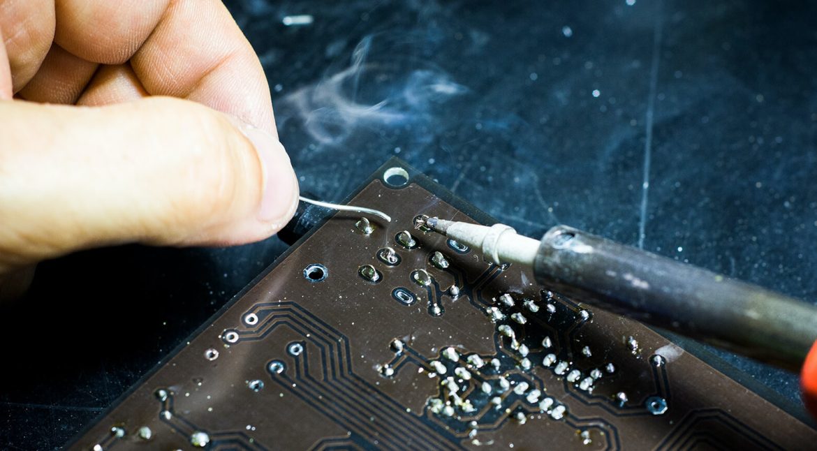
Where a terminal is soldered by hand, the process has to be specified: iron size, temperature, dwell time and the inspection that follows. A cold joint on a power terminal will heat up in service, and the failure it produces is a fire risk rather than a functional one.
Protection and Sensing
The board is also the place where protection is implemented: fuses, varistors, current sensing and the residual current detection that the standard requires. The layout of the sensing path affects the accuracy of the measurement and, in the case of a shunt, its temperature drift.
Sensing a large current with a shunt requires a Kelvin connection to the element, with the measurement traces taken from inside the pad rather than from the current path. The difference between the two layouts is a few percent of reading, which is enough to fail a metering specification.
Safety, Standards and Documentation
A charging product is certified against a standard that defines the creepage, clearance, isolation and test requirements. The design has to demonstrate those distances on every layer, and the documentation has to show where each one is achieved.
That documentation is not paperwork for its own sake. A certification body will ask how a distance is maintained under a transformer, across a slot and around a connector, and a drawing that answers the question in advance saves a round of questions later.
Assembly and Test
The assembly process has to handle heavy copper, large thermal masses and mixed technology on one board. Reflow may be followed by wave or selective soldering for the terminals, and each process has to be qualified for the thermal load it sees.
Testing covers insulation resistance, dielectric withstand, functional behaviour under load and the accuracy of the metering. The current capacity assumptions should be verified on a sample with a thermal measurement rather than accepted from a table, and the material choice confirmed against the guidance on high precision laminate and on metal core constructions.
High Voltage Layout Practice
On the high voltage side of the board, the routing is dominated by distance rather than by impedance. Conductors are kept apart to the distance the standard requires, and every layer is checked, because a plane that approaches the barrier on an inner layer defeats the separation achieved on the surface.
Test points and vias are part of the same calculation. A via on the mains side exposes copper at a defined distance from everything around it, and a test point that is probeable also has to be touch safe in the finished product.
EMC and the Switching Stage
The converter is a strong source of conducted and radiated emission. The input filter, the switching loop and the transformer all contribute, and the layout of the loop is what decides how much of the energy has to be filtered afterwards.
The principles are the same as for any switching supply, scaled up: keep the loop small, return the current to its source, and place the filter at the boundary of the board so that noise does not travel across it. The radiated emission behaviour of the switching stage is the same problem as in a small converter, with more current behind it.
FAQ
How much copper does a charger board need? It depends on the current and the permitted temperature rise. Many designs start at two ounces on the outer layers and add plating or a busbar as the current rises.
Why is a slot used for creepage? Because creepage is measured along the surface. A slot interrupts that path and increases the distance without adding board area.
Can a standard laminate be used? For the control section, usually yes. The power section normally needs a higher glass transition grade because of the temperature inside the enclosure.