Hybrid Multilayer PCB Price Guide: 2026 Cost Factors and Quotes
What a Hybrid Multilayer PCB Is
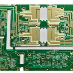
A hybrid multilayer PCB combines two or more dielectric materials in one laminated stack. The most common combinations are FR-4 with Rogers 4350B, FR-4 with Rogers 4003C, FR-4 with PTFE, FR-4 with Megtron 6, Rogers with PTFE, and FR-4 with ceramic filled high frequency material. The purpose of mixing materials is simple: the high speed and high frequency layers use a low loss laminate where signal quality matters, while the rest of the board uses lower cost FR-4 for power, control and grounding functions.
Hybrid stacks have become the mainstream solution for AI servers, 800G and 1.6T switches, 5G base stations, automotive millimeter wave radar, satellite communication and high speed data centers. Compared with building the whole board from Rogers or another premium laminate, a well designed hybrid structure usually saves 20 to 50 percent of the material cost while keeping the electrical performance of the critical layers. That balance is the reason buyers see so many hybrid quotations in 2026.
2026 Reference Price Ranges
Hybrid multilayer PCBs have no single market price because the mix of materials, layer count, size, process difficulty, impedance control, HDI structure and order quantity all affect the quote. As a practical guide for 2026, a four layer hybrid PCB in prototype quantity typically costs 120 to 250 US dollars including tooling; medium batches run from 35 to 70 dollars per board, and large production volumes can fall to roughly 12 to 25 dollars per board. A six layer hybrid stack adds about 40 to 60 percent on top of the four layer price at each quantity level, with prototypes often quoted at 200 to 400 dollars.
The gap between the cheapest and most expensive quotation for the same board outline is usually caused by the RF material content. A design that only needs a small Rogers island under a connector is far cheaper than one whose entire signal core is PTFE or Megtron. Buyers should always compare quotations that state the same material grades, the same number of RF layers and the same test plan, because otherwise the numbers are not comparable.
Material Selection Drives the Base Price
Material content is the largest single cost driver in a hybrid board. Rogers 4003C and 4350B are the most popular RF materials for hybrid stacks because they are rigid, easy to process and have stable dielectric constants around 3.4 to 3.7. PTFE offers very low loss for the highest frequencies but is soft, moisture sensitive and difficult to plate and drill, which raises fabrication cost and lowers yield. Megtron 6 and similar low loss materials are chosen for very high speed digital links rather than pure RF, and they also carry a premium over FR-4.
Hybrid designs should use the expensive material only where the signal actually needs it. A common layout places one or two low loss signal layers near the top of the stack, or a small RF section on one corner of the board, with FR-4 filling the remaining layers. Each extra RF layer adds significant cost, so the layer stack should be optimized together with the electrical simulation rather than copied from another project.
Layer Count and Stack Construction
Hybrid boards are usually four to ten layers, although AI server backplane style products can go higher. Every additional layer pair adds lamination, drilling, plating and inspection cost, and in a hybrid board the cost step between layer counts is larger than in an all FR-4 design because two different materials must be handled in the same lamination cycle. The position of the RF layers in the stack also matters: material transitions create stress and registration challenges, and the fabricator must manage the different coefficients of thermal expansion of FR-4 and high frequency laminates.
The transition between materials inside the board is where most manufacturing problems occur. The RF material and FR-4 expand and shrink differently during lamination, which can cause drill smear, pad shifts and delamination if the stack is not designed for the materials. A good fabricator reviews the stack with the customer before production and may recommend a specific order of layers or an additional prepreg stage to keep the materials stable.
Impedance Control and Signal Integrity
Hybrid boards are chosen for signals that ordinary FR-4 cannot carry, so impedance control is a core requirement rather than an option. Every high speed pair must be designed to a target impedance, verified with coupons, and held within tolerance across the panel. The dielectric constant and thickness of the RF material determine the trace geometry, and the fabricator’s etch and lamination capability decides how close the production board comes to the design value.
Signal integrity in a hybrid board also depends on the transitions. When a signal moves from the RF layer to an FR-4 layer, the change in dielectric constant changes the effective velocity and impedance; the design must provide continuous reference planes and consistent via structures so the transition does not create reflections. High speed design reviews at the layout stage catch these problems before the expensive hybrid board is ordered, which is why full service suppliers include DFM and stackup review in the quotation process.
Manufacturing Difficulty and Yield
Fabricating a hybrid multilayer board is harder than fabricating an FR-4 board of the same layer count. PTFE surfaces need special activation before plating, Rogers materials are abrasive to drills, and the different materials must be laminated with a cycle that suits both. Small variations in the process produce scrap, and because the material is expensive, the yield loss directly inflates the delivered price. Suppliers experienced with high frequency materials keep their yields high by controlling drilling parameters, plasma or chemical treatment, and lamination pressure profiles.
Surface finish on hybrid boards is usually immersion gold or another flat finish that suits high frequency signals and fine pitch assembly. The finish must also survive the environment of the final product, since many hybrid boards go into outdoor base stations or automotive modules. The finish choice is small in material cost but important in reliability, and it should be specified together with the assembly method.
Assembly and Testing Cost
Hybrid boards are often assembled in mixed technology with fine pitch BGAs, RF connectors and shielding. The assembly process must respect the frequency of the design and the sensitivity of the materials; soldering temperature, placement accuracy and cleaning all affect the RF performance. Boards with PTFE need careful handling because the material is soft and can be damaged by rough process steps.
Testing adds another cost layer. Bare boards need electrical test and impedance verification, and assembled boards need automated optical inspection plus functional or RF testing depending on the product. For 5G and radar modules, sample RF measurement of return loss and insertion loss is commonly required, and the records should follow the batch. Suppliers that combine fabrication with SMT PCB assembly and PCBA testing keep these records in one file, which simplifies qualification for the end customer.
How to Reduce the Cost of a Hybrid PCB
The most effective saving is minimizing the RF material content. Use low loss material only on the layers and areas where the signal requires it, and let the rest of the board remain FR-4. Second, standardize the stack and the board size across a product family so that panels are used efficiently and the fabricator can repeat a proven process; hybrid boards reward repetition because each new stack configuration needs its own process validation.
Third, reduce layer count where possible. A six layer hybrid board with careful routing may replace an eight layer design, saving lamination and material cost while keeping signal integrity. Fourth, choose mature materials. A slightly higher loss material that is easy to process can be cheaper in total cost than an exotic laminate with lower headline loss but poor yield.
Finally, order fabrication and assembly together. A single supplier that handles the PCB manufacturing and the assembly avoids the cost and risk of shipping expensive hybrid boards between factories, and it can optimize the stack and the panel with the assembly process in mind.
Getting a Reliable Hybrid Multilayer Quote
When requesting quotations for a hybrid multilayer board, send the Gerber files, the material list with grades, the layer stack, the impedance requirements and the expected volume. Ask the supplier to confirm that it has processed the specific material combination before, and to state its test plan for impedance and RF performance. A quotation that includes a DFM review of the stack and the transitions is more valuable than one that only repeats the layer count.
gopcb fabricates hybrid multilayer PCBs with FR-4, Rogers, PTFE and low loss digital materials, and assembles them with fine pitch SMT and RF aware processes under one roof. The engineering team reviews the stack, checks the material transitions and the impedance plan, and coordinates fabrication with assembly so the delivered boards match the design. Send gopcb your hybrid PCB design files and volume for a free DFM review and a 2026 quotation with material and test options.