Flexible Circuit Design Steps: How a Flex Board Is Built
A flexible circuit is designed around movement rather than around area, and that changes the order in which decisions have to be made. The bend comes first, the stackup follows, and the conductor geometry is derived from both. This guide walks through the steps of flexible circuit design in the sequence that avoids a redesign, and explains what each step costs.
How a Flexible Circuit Is Constructed
A flexible circuit is built on a thin polymer film, usually polyimide, with copper bonded to it either with an adhesive or directly in an adhesiveless construction. A coverlay, which is a second layer of film with openings for the pads, encapsulates the conductors and provides the mechanical protection that solder mask cannot give on a moving part.
That three-part sandwich, film, copper and coverlay, is the whole construction. Everything else, the stiffeners, the connectors and the plating, is added for a mechanical or an assembly reason. Understanding the sandwich makes it easier to see why each design step exists and what it affects.
Step One: Define the Bend Requirement
The first question is whether the circuit will bend once, in a static fold, or many times in a dynamic application. A static bend tolerates a tighter radius and a thinner specification, while a dynamic bend sets the minimum bend radius, the copper type and the number of layers the design can use at all.
The number of cycles belongs in the requirement as well. A flex that folds once during assembly and a flex that moves with a lid every day are different products, and the second one may not be achievable on a single copper layer if the cycle count is high.
Step Two: Choose the Flex Stackup
A single-sided flex is the most flexible and the cheapest, because the copper is on one face and the neutral axis can be placed inside the conductor. A double-sided flex doubles the routing capacity but moves the conductors away from the neutral axis, which reduces the achievable bend radius.
Multi-layer and rigid-flex constructions add further capability at a higher cost. A rigid-flex board lets a single part carry rigid component areas and a moving tail without a connector, and its flex stackup has to be designed so that the rigid sections do not intrude into the bend zone.
Step Three: Plan the Copper and the Coverlay
Rolled annealed copper is the normal choice for a dynamic bend because it tolerates repeated flexing far better than electrodeposited copper. It costs more and behaves differently in etching, so the decision should come from the bend requirement rather than from the price list. For a static fold, the cheaper foil is usually adequate.
The coverlay is the next decision. A laminated coverlay is inexpensive and robust; a photoimageable cover layer holds tighter openings and suits dense circuits. Both add a processing step, and the choice sets the minimum pad opening and therefore the component pitch the finished flex can accept.
<img src="https://www.gopcba.com/wp-content/uploads/2026/08/What-Is-Automotive-PCB.webp" alt="Flexible circuit cross section with stiffener and rolled annealed copper” />
Step Four: Lay Out the Bend Zone
The bend zone should contain conductors running perpendicular to the bend line, evenly spaced, with no plated holes and no abrupt changes in width. A conductor that runs along the bend, or a via placed inside it, becomes a crack initiation point. Where the design forces a hole near the bend, keeping it outside the zone and adding a stiffener is the usual answer.
Conductor width and spacing have to be balanced against flexibility. Wider conductors carry more current but resist bending, so the usual approach is to use several narrow traces in parallel rather than one wide trace. Applying manufacturable design guidelines to the bend zone prevents a layout that is buildable but not flexible.
Step Five: Add Stiffeners and Connectors
A stiffener is bonded behind the area where a connector or a component is mounted, so that the insertion force is taken by a rigid backing rather than by the film. Its thickness and its outline belong in the drawing, because a stiffener that extends into the bend zone changes the mechanical behaviour of the whole part.
Connectors add their own constraints. Zero-insertion-force types avoid stressing the flex, while a direct solder connection needs a stiffener and a defined strain relief. Zoned adhesion, where the coverlay is bonded selectively to keep the bend area compliant, is sometimes used to reduce stress at the transition.
Step Six: Plan Assembly and Test
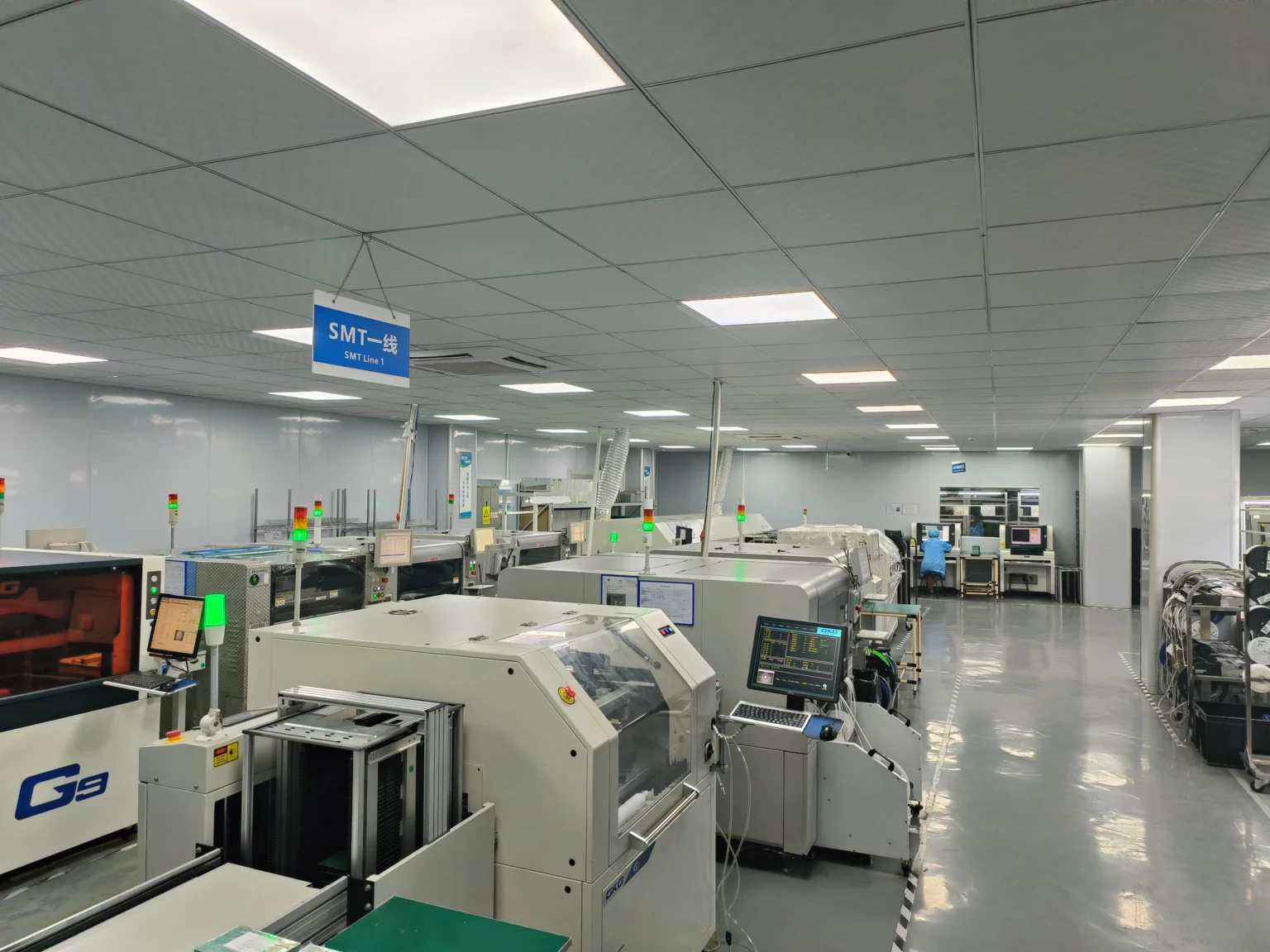
Assembly planning starts with handling. A flexible circuit cannot be processed on the same conveyor or in the same tray as a rigid board without support, so a carrier is normally used through printing, placement and reflow. That carrier is tooling, and it should be designed with the panel rather than after it.
Test access also has to be planned. A flex has no room for a large test pad field, so test points are usually grouped at the rigid end or on the connector pads. If the assembly will be tested with a fixture, the fixture needs mechanical support for a part that will not sit flat on its own.
Cost, Tooling and Prototype Sequencing
Cost is driven by the film, the number of lamination and bonding steps, the stiffeners and the coverlay process. A single-sided static flex is the cheapest construction, and each step away from it, double-sided, adhesiveless, multi-layer or rigid-flex, adds both cost and qualification work.
Tooling includes the coverlay artwork, the stiffener programme, a forming or bend fixture and often a carrier. None of those are expensive individually, and together they dominate a small prototype order. Building the first article on the production flex stackup avoids a second tooling cycle, which is why the sequence above matters more than any single decision in it.
Process Control and Verification
Reviewing the design before the data is released is far cheaper than correcting it after the panel is in the tank, because every step downstream inherits the decision made at the front end. Where a value sits close to a process limit, the drawing should say so, since the shop can then open the process window rather than working to a nominal figure that carries no tolerance.
The measurements that matter are the repeatable ones: conductor width and spacing, annular ring, finished hole size, plating thickness and surface finish are all verifiable on a coupon that travels with the panel. Documenting the assumption is part of the design work, and a short note on the drawing prevents a question that would otherwise arrive a day later and cost a day of schedule.
Related reading: our fabrication notes, board quality and design release notes cover the same ground.
FAQ
How tight can a flex bend radius be? A common planning figure for a dynamic bend is ten times the total thickness, and a static fold can often go considerably tighter. The correct value depends on the copper type, the layer count and the number of cycles, so it should be confirmed with the fabricator.
Do I need a stiffener on every flex? Only where a connector, a component or a test point needs mechanical support. A stiffener inside the bend zone does real harm, so the outline should be defined as carefully as the circuit itself.
Can a flexible circuit use standard surface mount assembly? Yes, with a carrier for handling and a reflow profile suited to the film. The thermal mass is much lower than a rigid board, so the profile is usually shorter and needs to be verified rather than assumed.