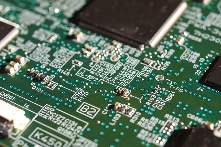
GPU PCB Design: Layer Counts, Materials and Signal Integrity
A graphics card is not a motherboard with a bigger chip on it. The GPU package carries thousands of solder balls, the memory sits on very short and carefully matched traces, and the power delivery section can pull hundreds of amps through a copper structure that also has to carry heat away. A GPU PCB is the combination of high layer count, fine geometry and heavy copper that makes all of that possible.
What Makes a GPU PCB Different
Three requirements collide on the same board. Signal integrity demands thin dielectric layers, controlled impedance and low loss material for the PCIe lanes and the memory bus. Power integrity demands thick copper, many parallel vias and a low impedance path from the regulators to the die. Thermal management demands that the copper which carries the current also conducts heat into the board and out to the backplate.
The usual answer is a high layer count stack with a mix of thin signal layers and thick power layers, built with HDI techniques that allow vias to be placed inside component pads. Entry level cards manage with six to eight layers; flagship and accelerator boards run twelve to twenty or more, with laser drilled microvias in the outer layers and mechanically drilled vias deeper in the stack.
Layer Count and Stackup Choices
Layer count follows the number of independent routing channels, not prestige. The memory bus needs matched length groups that are mostly routed on their own layers, the PCIe lanes need reference planes directly beneath them, and the power delivery needs at least one solid plane pair for each major rail. Once those are allocated, the remaining signal layers are counted from the pin density of the GPU package.
Where the count pushes past what mechanical drilling can serve, the stack moves to HDI and the via strategy becomes the design. Microvias stacked on buried vias, or staggered to avoid stacking, are the two common arrangements, and the choice affects both the achievable density and the fabrication yield. The trade-offs are the same ones described in via and stack selection.
Materials for High Speed and Heavy Copper
Standard FR4 is adequate for the lower speed lanes, but the loss budget on a PCIe 5.0 link at 32 GT/s is tight enough that most designs move to a low loss laminate for those layers. These materials lower the dissipation factor and hold impedance more stably over temperature, at a cost premium and with a different drilling behaviour that the fabricator has to account for.
Copper weight is the other material decision. One ounce copper is normal for signal layers, while the power section often uses two ounce or heavier copper to keep the voltage drop small and to spread heat away from the regulators. Heavy copper etches differently, so minimum line width and spacing on those layers are looser than on the signal layers, and the stackup has to reflect that.
Memory Interface and Signal Integrity
The bus between the GPU and its memory is the densest high speed structure on the board. Every byte lane is a group of traces that must arrive together, so length matching within a group is a hard requirement, and the groups must be matched to each other as well. Reference planes have to be continuous under the whole bus, because a split in the plane turns a matched trace into a discontinuity.
Crosstalk is the second constraint. The traces run close together for their whole length, so the spacing rule and the plane clearance are set by the coupling budget rather than by the manufacturing minimum. Where the routing has to change layer, the via stub is removed by backdrilling, because a stub that is a fraction of a wavelength long will degrade the channel at the top of the frequency range. The underlying spacing rule is described in crosstalk and the 3W rule.
Power Delivery and Thermal Path
The regulator section on a modern card is a multiphase converter delivering hundreds of amps at close to a volt, and the board is part of the circuit. Each phase needs a low impedance path to the die, which means multiple vias under each pad, generous copper area and a plane pair that keeps the loop inductance small. The conductors that carry the current are sized on the same basis as any other high current trace, as covered in trace width and current.
Thermally, the board is a heat spreader as much as a circuit. Thermal vias under the GPU and under the regulator array move heat into the inner copper and out to the backplate, and the copper distribution is deliberately balanced to avoid hotspots. Warpage is the failure mode to watch: a large card with heavy copper on one side and a heavy cooler bolted to it will bow unless the copper is distributed evenly and the stackup is symmetrical.
Assembly and Inspection Expectations
The GPU package is a large area array device, and the assembly process has to hold the whole array within a few tens of microns while the board itself may move slightly at reflow temperature. That places demands on stencil design, on the reflow profile and on board flatness, and it is why inspection is done with X-ray rather than optically for the package balls.
Impedance and loss are verified with coupons on the production panel, not by assumption. A high speed design that passes continuity test can still fail the link budget if the dielectric thickness drifted or the etch factor changed, so time domain reflectometry coupons and insertion loss coupons are normally part of the fabrication specification for anything running above a few gigahertz.
Common Failure Modes
Warpage tops the list because it is slow and thermal. A card that is flat at build can bow after a few hundred power cycles, and the consequence is a cracked solder ball under the package rather than an obvious board defect. Copper balance, symmetric stackups and a stiffener or backplate that does not itself distort the board all address it.
Regulator failures are the second group. Inadequate copper, insufficient vias or a poorly placed thermal path will raise the local temperature until a MOSFET or the board itself fails. Signal margin failures are the third: a link that trains at reduced speed or drops under load usually traces back to a reference plane discontinuity, an unmatched length group or an impedance that drifted outside tolerance.
Specifying a GPU Board
A workable specification states the layer count and stackup, the material for each signal group, the copper weight per layer, the impedance targets and tolerances, the via strategy including whether backdrilling is required, and the flatness requirement. Vague specifications produce boards that meet the drawing and still fail in the chassis, because the properties that matter on a high speed card are not visible on a mechanical outline.
It is worth confirming fabrication capability before the layout is fixed, particularly for HDI with heavy copper and for controlled depth backdrilling. The combination is not offered by every fabricator, and discovering that after the layout is complete means either a redesign or a longer supply chain. High frequency routing practice is covered in high frequency trace routing.
FAQ
How many layers does a GPU PCB need? Entry level gaming cards use six to eight layers, mid range cards use ten to twelve, and accelerator or server boards commonly exceed twenty. The count follows the memory bus width, the power delivery structure and the pin count of the package.
Why is a GPU board so much more expensive than an ordinary multilayer board? Because it combines a high layer count, low loss material, HDI vias, heavy copper and tight impedance control on one panel, and each of those reduces yield and increases process time.
Can a damaged GPU board be repaired? Simple faults such as a failed capacitor or a single regulator phase can often be reworked. Damage inside the multilayer structure, cracked BGA balls or delamination under the die cannot be repaired reliably and the card is scrapped.