HDI Any Layer Stackup Selection
An any layer HDI board is one in which a microvia may be formed between any two adjacent layers, including the connections between the outer layer and the layer beneath it and between two inner layers. That freedom is what allows a dense device fanout on a board with many layers, and it is bought with a build cycle in which each pair of layers is laminated and drilled in turn.
This article describes what the construction means, how the sequential lamination steps accumulate, and how the stack and the via arrangement should be chosen.
What Any Layer Means
In a conventional multilayer board the vias pass through the whole thickness, so every signal that changes layer occupies a hole through every layer beneath it. In an HDI board the vias are blind or buried and connect only two adjacent layers, which frees the space that the through holes would have taken. When that principle is applied to every layer pair, the board is described as any layer, and the routing capacity rises sharply because each connection consumes only the two layers it joins.
The cost is in the build. A board with eight layers and vias between every pair is laminated four times, once for each pair, with a drilling and plating step between the laminations. Each additional cycle adds yield loss, adds process time, and adds a risk that a panel already partially built will be scrap. The decision to use any layer is therefore a decision about routing density versus cost and yield, and it is normally taken only when the device pitch and the pin count leave no alternative. The construction itself is defined by the layer arrangement, as described under layer stackup from one to eight layers.
Sequential Lamination Steps
The build starts with a core carrying the inner layer pattern, with copper on both faces. A dielectric layer is laminated on each side, a thin copper foil is applied over it, and the microvias are drilled through the dielectric to the core pattern below. The foil is then plated and patterned to form the next layer, and the sequence repeats. Because each cycle adds only one layer on each face, the layer count grows in pairs, and an odd final count is not achievable by this route without a specific construction.
Two parameters are fixed at the start and are difficult to change later. The first is the dielectric thickness of each build-up layer, which sets the depth of the microvia. The second is the copper thickness on the layers that will be drilled, because the laser has to stop on a copper pad that is thick enough to survive the process. Both determine the drilling window and both are recorded in the fabrication drawing rather than left to the shop. The data preparation for such a build, including the compensation of each lamination, is described under HDI CAM methods.

Via Stack Options And Trade-offs
Within an any layer construction the vias may be arranged in three ways. They may be staggered, so that each via lands on a pad offset from the one below and the connection walks across the board. They may be stacked directly, so that one microvia sits on the copper of the one beneath and the connection is a vertical column. Or they may be stacked with a copper filled pillar in the lower via so that the upper via lands on solid metal.
A staggered arrangement is the most forgiving and the least dense, because each via needs its own pad and the offset consumes routing space. A direct stack saves the most space and concentrates the most stress at one point, so the pads at the bottom of the stack see the accumulated strain of every layer above. Filling the lower via with copper before the next lamination spreads the load and allows deeper stacks, and the plating parameters that make that fill reliable are covered under electroplating and via filling for HDI. The choice among the three arrangements, and the limits on how many vias may be stacked, are described under blind and buried via stack selection.
Core Thickness And Aspect Ratio
A microvia is drilled only through one build-up dielectric layer, so its aspect ratio is low and the plating chemistry reaches the bottom easily. The same is not true of the through holes that remain in the finished board, which now pass through the core and every build-up layer together, and those holes have the full board thickness to cross. An any layer board with a thick core can therefore combine easy microvias with difficult through holes, and the through hole is often the plating step that limits the design.
The core thickness is also what gives the finished board its stiffness and its dimensional stability. Making the core thin to reduce the through hole aspect ratio makes the board flexible, which complicates handling through the lamination cycles, and it reduces the ability of the panel to hold registration across repeated builds. The usual compromise is a core thick enough to handle and thin enough that the through holes remain within the plating window, with the build-up layers kept as thin as the drilling process allows.
Where The Yield Goes
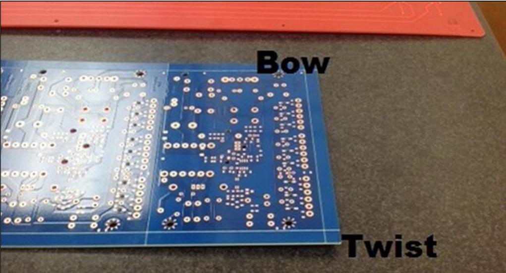
Each lamination cycle is a chance to lose a panel, and the losses compound. A panel that has passed three build cycles and fails at the fourth carries the cost of all three. The loss mechanisms differ by cycle as well: the first cycles lose panels to drilling defects and to dielectric voids, while the later cycles lose panels to damage from handling and to warpage that grows as the stack becomes asymmetric.
Two controls keep the loss manageable. The first is testing the panel at an intermediate stage, so that a panel that is already defective is removed before more value is added. The second is to keep the construction as symmetrical as possible in both copper distribution and dielectric thickness, so that the panel does not build in a warp that appears only after the final lamination. Symmetry in a stack is discussed in the context of layer counting under balanced stackup and odd layer count.
Choosing Between HDI Types
An any layer board is at one end of a range. At the other end a conventional board with through holes and no microvias is the cheapest and the slowest to route. Between them lie constructions with one build-up cycle on each face, or with microvias only on the outer layers, or with buried vias in the core. Each step up the range adds a lamination cycle and removes a layer of routing congestion.
The choice is made by counting connections rather than by preference. If the device fanout fits without microvias, the conventional board is correct. If one build-up cycle on each face resolves the congestion, there is no reason to move to any layer. The move is justified only when the number of connections that must change layer within a small area exceeds what a single microvia layer can carry, and the cost of the extra cycles is then the price of the package pitch rather than an optional refinement.
FAQ
Is any layer HDI the same as every layer HDI? The terms are used interchangeably in most practice, and both mean that a microvia may be formed between any two adjacent layers. Some suppliers reserve one of the terms for a construction in which every layer pair carries microvias, so the drawing should state the requirement in terms of the via types used, not only with a label.
How many vias may be stacked in one column? It depends on the pad size, the fill quality and the product specification. A direct stack of two or three microvias is common; beyond that, the lower vias are normally copper filled to spread the load, and the limit is established by thermal cycling data for the specific construction.
Why does any layer reduce routing congestion so much? Because each connection occupies only the two layers it joins. On a conventional board a signal that moves from the top layer to an inner layer consumes a hole through every layer below, and those holes block routing on all of them.