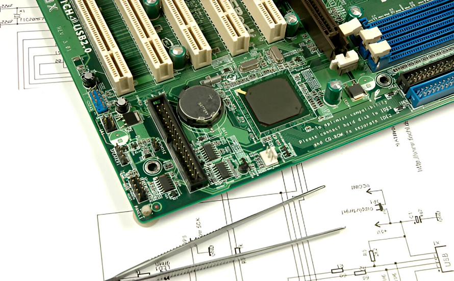
PCB DFM: Design for Manufacturability Guidelines for PCB Design and Manufacturing
During the planning stage of a new electronic product, both the technical and financial aspects of PCB Manufacturing must be carefully considered. Keeping manufacturing costs under control is particularly important for high-volume production, where even a small design issue can increase material consumption, production time, and rework costs.
A PCB design that requires repeated modifications can also affect the overall project schedule and profitability. To minimize these risks, engineers should develop the PCB layout with manufacturing requirements in mind from the beginning.
After receiving the CAM data, a PCB manufacturer may identify minor design issues that need to be corrected before production. Although these issues may appear insignificant, repeated changes can result in additional engineering work, manufacturing delays, and unexpected costs.
This is why PCB Design for Manufacturability (DFM) is an essential part of modern electronics development. By applying DFM principles during the PCB layout stage, engineers can identify potential manufacturing problems before the design reaches production.
This article explains the most common PCB DFM issues and provides practical guidelines that can help improve the electrical, mechanical, thermal, and manufacturing performance of a PCB.
What Is DFM in PCB Design?
DFM stands for Design for Manufacturability. In PCB development, DFM refers to designing a circuit board in a way that allows it to be manufactured efficiently, consistently, and reliably using the intended production processes.
PCB DFM bridges the gap between an electronic design and the physical manufacturing process. Instead of designing a PCB based solely on electrical requirements, engineers also consider manufacturing tolerances, minimum feature sizes, component placement, drilling, copper distribution, soldering, assembly, inspection, and testing.
A typical PCB DFM checklist may include:
- Minimum trace width and spacing
- Minimum hole and microvia dimensions
- Copper-to-edge clearance
- Component-to-component spacing
- Solder mask clearance
- Silkscreen placement
- Pad and footprint geometry
- Via design
- Copper distribution
- PCB panelization
- Thermal management
- Assembly accessibility
- Manufacturing tolerances
The actual values should always be based on the capabilities of the selected PCB manufacturer and the applicable industry standards.
PCB DFM is also a cross-functional process. PCB designers, electrical engineers, mechanical engineers, manufacturing engineers, component engineers, and PCB manufacturers may all contribute to the final design review.
Why Is PCB DFM Important?
A PCB can be electrically functional in a CAD environment but still be difficult or expensive to manufacture.
For example, a design may contain traces that are too narrow, clearances that are too small, incorrectly designed footprints, insufficient copper spacing, or components positioned too close to the board edge.
If these issues are discovered late, engineers may need to modify the layout and regenerate manufacturing files. In high-volume production, such changes can affect both manufacturing efficiency and product cost.
Applying DFM early provides several benefits:
- Reduces manufacturing defects
- Minimizes design revisions
- Improves production yield
- Reduces manufacturing costs
- Simplifies PCB assembly
- Improves inspection efficiency
- Enhances electrical and mechanical reliability
- Shortens the transition from design to production
For these reasons, DFM should not be treated as a final inspection step. It should be integrated into the entire PCB Design workflow.
Common PCB DFM Problems

Some DFM problems can be detected during PCB layout, while others may only become apparent when manufacturing engineers review the CAM data.
Ignoring these problems can lead to low production yields, additional engineering work, assembly defects, or even field failures.
The following are some of the most common PCB DFM issues.
1. Incorrect Component Footprints
Every electronic component used in a PCB design requires an appropriate footprint in the PCB library. The footprint defines the pad geometry, spacing, component outline, soldering area, and other physical characteristics required for PCB assembly.
An incorrect footprint can result in poor solder joints, component misalignment, insufficient pad area, or even complete assembly failure.
Engineers should therefore verify that footprints correspond to the actual component package and recommended land pattern. Industry standards such as IPC guidelines can be used as references when creating or reviewing footprints.
Where available, standardized footprint libraries and verified CAD library tools can significantly reduce footprint-related errors.
For complex or fine-pitch components, the footprint should also be checked against the component manufacturer’s recommended land pattern.
2. Poor Component Placement
Component placement is one of the most important aspects of PCB Design for Manufacturability.
During layout, designers should consider:
- Component-to-component clearance
- Component height
- Board-edge clearance
- Connector accessibility
- Heat-generating components
- Assembly orientation
- Rework accessibility
- Inspection requirements
- Mechanical interference
Components should not be placed too close to the PCB edge because they may interfere with depanelization, handling, fixtures, or assembly equipment.
Connectors, switches, power interfaces, and other user-accessible components should also be positioned according to the mechanical design of the final product.
Good component placement improves not only manufacturability but also thermal performance, signal integrity, and serviceability.
3. Soldering and Assembly Problems
After the PCB layout passes the DFM review, the next major consideration is PCB assembly.
Component pad geometry and placement must be compatible with the selected soldering process. Poor pad design or inappropriate component spacing can contribute to solder bridges, insufficient solder joints, component misalignment, and other assembly defects.
One common example is tombstoning, in which a small passive component such as a resistor or capacitor becomes lifted on one end during reflow soldering.
Tombstoning can be influenced by several factors, including:
- Unequal pad sizes
- Uneven solder deposition
- Differences in thermal balance
- Incorrect component placement
- Unequal copper distribution
- Improper stencil design
- Reflow profile conditions
Therefore, pad geometry and component placement should be optimized for the actual SMT assembly process rather than simply following the schematic connection.
For fine-pitch components, designers should also maintain appropriate solder mask and pad-to-pad clearances to minimize the risk of solder bridging.
4. Floating or Unconnected Copper

Unconnected copper areas can create manufacturing and electrical concerns if they are not intentionally designed.
During PCB layout, designers should carefully review isolated copper islands around vias, pads, traces, and polygon areas.
Unconnected copper can potentially behave as an unwanted capacitive structure or antenna, particularly in sensitive high-frequency designs. It can also create uneven copper distribution, which may contribute to manufacturing challenges.
Antenna Effects
A floating copper area may pick up or radiate unwanted electromagnetic energy depending on its geometry, surrounding structures, and operating frequency.
This can become particularly important in RF and high-speed circuits, where signal integrity and electromagnetic compatibility are critical.
Designers should therefore ensure that copper regions are intentionally connected to an appropriate net or removed when they provide no functional benefit.
Copper Slivers
Very narrow copper features can be difficult to manufacture consistently.
During PCB etching, extremely thin copper features may not maintain sufficient mechanical strength or dimensional stability. They can become partially detached or create unwanted conductive debris.
To prevent this problem, designers should define appropriate minimum copper widths and clearances according to the capabilities of the PCB manufacturer.
A reliable PCB DFM process should eliminate unnecessary copper slivers before manufacturing data is released.
5. Sharp Copper Corners
Sharp corners in PCB traces can create manufacturing and signal-integrity concerns.
Historically, designers were often advised to avoid 90-degree trace corners because of concerns about acid traps during etching. Modern PCB manufacturing processes can accommodate 90-degree corners in many situations, so they are not universally prohibited.
Nevertheless, unnecessary acute-angle corners should generally be avoided. Using 45-degree corners or curved routing can produce a cleaner layout and may be preferable for high-speed and RF designs.
The most important consideration is to follow the manufacturer’s routing and manufacturing guidelines rather than applying an outdated rule without considering the actual fabrication process.
Designers should configure the appropriate routing rules in their ECAD tools before beginning PCB layout.
6. Unplated or Poorly Plated Holes
Vias and plated through-holes provide electrical connections between different PCB layers. Reliable hole metallization is therefore essential for multilayer PCB performance.
Problems such as incomplete copper plating, voids, insufficient plating thickness, or poor hole-wall quality can result from manufacturing process problems, unsuitable materials, contamination, or inadequate process control.
These defects may increase electrical resistance or cause intermittent or open connections.
To reduce this risk, designers should specify realistic hole dimensions and plating requirements that are compatible with the manufacturer’s capabilities.
For demanding applications, PCB manufacturers may use cross-section analysis and other quality-control methods to verify plated-hole reliability.
7. Via-in-Pad Design

Placing a via directly inside a component pad can provide excellent routing density, particularly for fine-pitch BGA and other high-density packages.
However, via-in-pad technology requires appropriate manufacturing control.
If an open via is placed directly in a solder pad, solder may flow into the via during reflow. This can reduce the amount of solder available for the component joint and potentially create an unreliable connection.
For this reason, via-in-pad designs often require processes such as via filling and planarization.
Engineers should not use via-in-pad simply to save routing space. They should first confirm that the PCB manufacturer can support the required process and tolerances.
8. Insufficient Solder Mask Clearance
Fine-pitch components such as processors, controllers, and other high-density ICs may have very small distances between adjacent pads.
If solder mask openings are not correctly designed, excessive exposed copper can increase the risk of solder bridging during reflow.
The solder mask design should therefore provide appropriate separation between adjacent pads while maintaining sufficient solderable area.
Solder mask also protects exposed copper from environmental contamination and helps reduce the risk of accidental solder connections between neighboring conductors.
For advanced PCB designs, solder mask expansion, dam width, registration tolerance, and pad geometry should be considered together.
How to Avoid DFM Errors in PCB Design
The ultimate objective of PCB DFM is to ensure that a design can move smoothly from engineering development to reliable mass production.
A systematic DFM review should therefore be performed before manufacturing files are released.
1. Verify PCB Footprints
Confirm that every component footprint matches the actual package and manufacturer’s recommended land pattern.
Special attention should be given to:
- Fine-pitch ICs
- BGAs
- QFNs
- Connectors
- Power components
- High-current terminals
- Through-hole components
2. Standardize PCB Panelization
PCB panelization should be planned according to the manufacturing and assembly process.
A well-designed panel can improve material utilization, simplify handling, and increase production efficiency.
Designers should consider:
- Board orientation
- Tooling rails
- Fiducial marks
- Breakaway methods
- V-score requirements
- Tab routing
- Component clearance from the panel edge
The goal is to achieve efficient panel utilization without compromising PCB quality or assembly reliability.
3. Keep the PCB Outline Manufacturable
The board outline should be designed according to the selected fabrication and depanelization process.
Unnecessarily complex outlines can increase machining time and manufacturing costs.
Where possible, designers should use simple and manufacturable board geometries while ensuring that the PCB fits the mechanical enclosure.
4. Run DRC and DFM Checks Before Release
A final PCB DFM checklist should be completed before manufacturing files are submitted.
Designers should verify:
- Trace width
- Trace spacing
- Copper-to-edge clearance
- Hole size
- Hole-to-copper clearance
- Solder mask clearance
- Silkscreen placement
- Component spacing
- Board outline
- Via structures
- Copper distribution
- Layer stackup
- Manufacturing tolerances
Both automated design-rule checking and manufacturer-side DFM analysis can be useful.
5. Maintain Uniform Copper Distribution
Uneven copper distribution can affect PCB fabrication and dimensional stability.
Large differences in copper density between different areas of a board can contribute to uneven etching, plating variation, and warpage.
Where appropriate, copper balancing techniques can be used to create a more uniform copper distribution across the PCB stackup.
6. Consider Component-Side and Soldering Requirements
Component placement should be compatible with the selected assembly technology.
For example, combining SMT and through-hole components may require additional soldering processes depending on the product architecture.
Rather than applying a universal rule such as placing all through-hole components on one side and all SMT components on the other, designers should evaluate the actual assembly sequence and manufacturing capabilities.
The goal is to minimize unnecessary process steps while maintaining reliable solder joints.
7. Use Teardrops Where Appropriate
Teardrops can be added at the junction between traces and pads or vias.
They gradually increase the copper width near the connection point, which can improve routing robustness and tolerance to manufacturing misalignment.
Teardrops can be particularly useful for high-density PCB layouts and designs with tight drilling or registration requirements.
8. Ensure SMD Connections Are Inspectable
When traces are routed from SMD pads toward dense internal areas, designers should consider whether the resulting solder joints and copper connections can be inspected effectively.
The layout should provide sufficient access for AOI and other inspection technologies whenever practical.
This is especially important for high-density components, where poor visibility can make manufacturing defects more difficult to detect.
9. Keep Silkscreen Text Clear
Silkscreen markings should not overlap component pads, solder mask openings, or other critical features.
Reference designators and polarity indicators should remain legible and correctly positioned.
Clear silkscreen information helps operators identify components and orientations during assembly, inspection, and rework.
10. Design Thermal Vias Correctly
Thermal vias can transfer heat from high-power components to internal copper planes or other thermal structures.
However, exposed vias inside solder pads may cause solder to drain away during reflow if they are not properly filled or otherwise designed for the assembly process.
Therefore, thermal-via structures should be coordinated with the component footprint, solder paste design, PCB stackup, and assembly process.
11. Calculate Trace Width and Clearance
Trace width should be selected according to the expected current, allowable temperature rise, copper thickness, and applicable design requirements.
After determining the required trace width, designers should also verify the clearance between the trace and other conductive features.
These values should then be incorporated into the ECAD design rules so that potential violations can be detected automatically during layout.
PCB DFM Checklist
A practical PCB DFM checklist can be summarized as follows:
| DFM Item | Key Consideration |
|---|---|
| PCB footprint | Verify package and land pattern |
| Component placement | Maintain appropriate clearance |
| Trace width | Match current and manufacturing requirements |
| Trace spacing | Follow voltage and fabrication requirements |
| Hole size | Match drilling capabilities |
| Via design | Consider reliability and assembly |
| Via-in-pad | Use filling/planarization when required |
| Solder mask | Maintain appropriate clearance and dam width |
| Silkscreen | Keep text clear and readable |
| Copper distribution | Avoid significant copper imbalance |
| Board outline | Ensure compatibility with fabrication |
| Panelization | Optimize material utilization and assembly |
| Thermal design | Provide appropriate heat dissipation |
| Inspection | Consider AOI and test accessibility |
| Manufacturing files | Verify Gerber/ODB++ and drill data |
Conclusion
Following PCB DFM principles is essential for transforming a PCB design into a reliable, manufacturable product.
DFM is not simply a final inspection performed before sending Gerber or other manufacturing data to a supplier. It should be incorporated throughout the PCB development process, from component selection and footprint creation to component placement, routing, stackup design, panelization, and final manufacturing-data review.
By addressing common issues such as incorrect footprints, poor component placement, inadequate clearances, floating copper, copper slivers, inappropriate via-in-pad structures, insufficient solder mask clearance, and uneven copper distribution, engineers can reduce manufacturing problems and improve production consistency.
For both simple prototypes and complex industrial electronics, an effective PCB Design and DFM workflow can help reduce unnecessary revisions, improve PCB assembly efficiency, support stable mass production, and control overall manufacturing costs.
As PCB technologies continue to evolve, engineers should also regularly update their PCB DFM checklist based on new manufacturing processes, materials, component packages, and the capabilities of their manufacturing partners.
Article Summary
PCB DFM, or Design for Manufacturability, is a critical part of modern PCB Design and PCB Manufacturing. It ensures that a circuit board is not only electrically functional but also practical, reliable, and cost-effective to manufacture. By checking footprints, component placement, trace geometry, vias, solder mask, copper distribution, thermal structures, panelization, and manufacturing files before production, engineers can reduce design revisions and manufacturing defects. A well-established PCB DFM process ultimately helps create more reliable products while improving production efficiency and controlling manufacturing costs.