What Is HDI PCB?
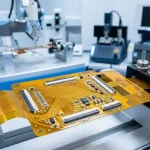
HDI PCB stands for High-Density Interconnect Printed Circuit Board. Unlike conventional PCBs that primarily rely on mechanical drilling, HDI technology uses precision laser drilling to create smaller microvias and enables finer traces and spacing. This allows significantly more circuitry to be integrated into a smaller board area.
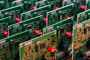
HDI technology is particularly suitable for modern electronic products that require compact dimensions, high component density, and reliable high-speed signal transmission. By using microvias, blind vias, buried vias, fine-line circuitry, and sequential buildup structures, an HDI PCB Manufacturer can help designers achieve greater routing density without continuously increasing the physical size of the circuit board.
HDI technology is widely used with high-density packages such as BGA, CSP, QFP, and other fine-pitch components. It has become an important PCB technology for smartphones, communication equipment, medical electronics, automotive electronics, industrial equipment, and other advanced electronic products.
For broader PCB production requirements, GOPCBA also provides comprehensive PCB Manufacturing Services covering standard, multilayer, HDI, flexible, rigid-flex, aluminum, and other specialized PCB technologies.
How Is HDI PCB Different From Conventional PCB?
Smaller Size and Higher Circuit Density
One of the primary advantages of High-Density Interconnect PCB technology is its ability to increase circuit density without significantly increasing board dimensions.
HDI boards use sequential buildup structures, microvias, and fine-line routing to make more efficient use of available PCB space. This makes it possible to design thinner, lighter, and more compact electronic products.
For portable and space-constrained applications, HDI technology can reduce PCB size while maintaining the required electrical and mechanical functionality.
Microvias and Laser Drilling
Traditional PCBs commonly use mechanically drilled through-holes. HDI PCBs, in contrast, incorporate laser-drilled microvias that can be significantly smaller than conventional mechanical holes.
Typical HDI manufacturing may involve microvia diameters around 0.075–0.10 mm depending on the board structure and manufacturing capability. GOPCBA’s published PCB capability includes laser-drilled microvias down to 0.08 mm in advanced HDI production.
Microvias can connect adjacent layers efficiently and free valuable routing space for high-density circuit designs.
Fine Trace and Spacing
HDI PCB designs require finer trace widths and spacing than many conventional PCB designs.
Fine-line technology allows designers to route more signals within the same area and provides greater flexibility when placing high-density components. GOPCBA’s published capabilities support advanced PCB structures with outer-layer trace/spacing down to approximately 64/76 μm and inner-layer trace/spacing down to approximately 50/50 μm.
The actual achievable trace width and spacing should always be determined according to the selected material, copper thickness, layer structure, board size, and production requirements.
High Pad and Component Density
HDI technology is particularly useful when a PCB contains high-pin-count components, fine-pitch BGAs, CSP packages, or other space-sensitive devices.
Microvias allow electrical connections to be routed directly from component pads or nearby copper features to adjacent layers. This reduces the routing limitations associated with conventional through-hole vias and creates more usable PCB space.
Thin Dielectric Layers
HDI construction generally uses thin dielectric materials between buildup layers. The reduced dielectric thickness supports high-density routing and can also contribute to controlled impedance designs.
For high-speed applications, dielectric thickness, copper thickness, trace geometry, material properties, and layer stack-up must be carefully controlled to achieve the required impedance and signal performance.
Electrical and Performance Advantages of HDI PCB
A well-designed Microvia PCB can provide several important electrical and mechanical advantages.
Improved Signal Integrity
Shorter interconnections and optimized via structures can reduce unwanted electrical effects associated with long signal paths. This is particularly important for high-speed digital interfaces, RF circuits, communication equipment, and advanced computing hardware.
Reduced Parasitic Effects
Compared with conventional through-hole structures, microvias can provide shorter electrical paths and smaller via structures. This can help reduce parasitic capacitance and inductance in high-speed designs.
Better EMI and EMC Performance
The compact routing structure of an HDI PCB can help engineers optimize signal paths, power distribution, grounding, and return paths. Proper stack-up design can therefore contribute to better electromagnetic compatibility and reduced interference.
More Efficient Thermal and Mechanical Design
HDI technology can reduce board size and provide greater freedom for component placement. This can help product engineers optimize the overall mechanical layout and thermal architecture of compact electronic systems.
For customers requiring different PCB structures, GOPCBA also supports PCB Capabilities including multilayer, HDI, high-TG, thick copper, high-frequency, impedance-control, blind/buried via, metal-base, and other advanced PCB technologies.
HDI PCB Structure and Classification
Blind Vias
A blind via connects an outer layer to one or more internal layers without passing completely through the PCB.
Blind vias are commonly used in HDI designs to improve routing density around high-pin-count components.
Buried Vias
A buried via connects internal PCB layers without extending to the external surface. Buried vias can provide additional routing flexibility in complex multilayer structures.
Microvias
Microvias are small-diameter vias generally produced using laser drilling. They are one of the defining technologies of modern HDI PCB construction.
Depending on the design, microvias can be arranged as staggered or stacked structures.
Stacked and Staggered Microvias
Stacked microvias are vertically aligned across multiple buildup layers, while staggered microvias are offset from one layer to another.
The appropriate structure depends on electrical requirements, component density, reliability targets, manufacturing capability, and cost considerations.
Copper-Filled Microvias
Copper filling can be used to improve microvia reliability and enable advanced structures such as via-in-pad. Proper copper filling and planarization are particularly important for fine-pitch BGA and other high-density component applications.
HDI PCB Manufacturing Process
The HDI PCB Manufacturing process requires tighter process control than conventional PCB production. A typical production flow may include:
- Material preparation and cutting
- Inner-layer imaging
- Inner-layer etching
- Layer inspection
- Lamination
- Mechanical drilling
- Laser drilling
- Desmear and surface preparation
- Electroless copper plating
- Pattern plating
- Microvia filling when required
- Outer-layer imaging and etching
- Solder mask application
- Surface finishing
- Silkscreen printing
- Electrical testing
- Final inspection
- Packaging and shipment
The exact process varies according to the HDI structure, number of buildup layers, material system, via design, copper thickness, and required surface finish.
GOPCBA provides PCB manufacturing from prototype development through volume production and supports technologies including blind vias, buried vias, plugged vias, impedance control, custom stack-ups, and HDI structures.
HDI PCB Manufacturing Capabilities
GOPCBA’s published PCB capabilities include standard and advanced HDI manufacturing options. Depending on the design and production requirements, capabilities include:
- Up to 48 PCB layers
- Fine-line trace and spacing
- Laser-drilled microvias
- Blind and buried vias
- Stacked microvias
- Copper-filled microvias
- High-density interconnect structures
- Controlled impedance
- Custom PCB stack-ups
- High-TG materials
- High-frequency materials
- Flexible and rigid-flex PCB technologies
For advanced HDI projects, the final capability should be confirmed through engineering review because achievable dimensions depend on board construction, materials, copper thickness, aspect ratio, and production volume.
Applications of HDI PCB
Consumer Electronics
HDI PCBs are widely used in compact consumer electronics where space, weight, and circuit density are critical.
Typical applications include smartphones, wearable devices, portable electronics, cameras, and other compact products.
Communication Equipment
High-speed communication equipment requires dense routing and reliable signal transmission. HDI technology is suitable for communication modules, networking equipment, RF systems, and high-speed electronic platforms.
Automotive Electronics
Modern vehicles contain increasingly sophisticated electronic systems, including ADAS, infotainment, connectivity, sensors, control units, and other electronic modules. HDI technology helps manufacturers integrate more functionality into limited physical space.
Medical Electronics
Medical devices often require compact, reliable, and highly integrated electronics. HDI PCBs can support miniaturized medical equipment, diagnostic systems, monitoring devices, and portable medical electronics.
Industrial Electronics
Industrial control systems, automation equipment, machine vision, robotics, and embedded computing platforms can benefit from high-density PCB technology when complex circuits must fit into compact enclosures.
GOPCBA also provides Industrial PCB Assembly solutions for industrial applications requiring rigid, flexible, and rigid-flex PCB technologies.
HDI PCB Assembly Considerations
HDI PCB manufacturing is only one part of the electronics production process. High-density boards often use fine-pitch BGA, CSP, QFN, 01005, and other advanced components, making assembly process control equally important.
A suitable manufacturing partner should therefore be able to support PCB fabrication, component sourcing, SMT assembly, inspection, testing, and production engineering.
GOPCBA provides PCB Assembly Services covering rigid PCB, flexible PCB, rigid-flex PCB, multilayer PCB, HDI PCB, heavy copper PCB, metal-core PCB, high-TG PCB, high-frequency PCB, and controlled-impedance PCB assembly.
Quality Control for HDI PCB
High-density PCB production requires strict process control because small variations in drilling, plating, lamination, registration, copper thickness, and solder mask alignment can affect final board performance.
Important quality-control procedures may include:
- Automated optical inspection
- Electrical testing
- Microsection analysis
- Via and plating inspection
- Dimensional inspection
- Impedance testing
- Solder mask registration inspection
- Surface finish inspection
- Final visual inspection
For prototype and low-volume projects, engineering review is also important. Design-for-manufacturing analysis can identify potential issues before production begins and reduce unnecessary design revisions.
GOPCBA provides engineering support including DFM review, DFA analysis, BOM verification, Gerber review, component availability analysis, prototype support, and manufacturing process optimization.
Choosing the Right HDI PCB Manufacturer
When selecting an HDI PCB Manufacturer, customers should evaluate more than the basic PCB price. Important factors include:
- HDI layer and buildup capability
- Minimum microvia size
- Trace and spacing capability
- Stacked and staggered microvia capability
- Copper-filled via technology
- Material selection
- Controlled impedance capability
- Prototype and mass-production capacity
- Electrical and reliability testing
- Engineering support
- Quality management
- Delivery performance
A capable supplier should be able to review the complete Gerber package, drill files, stack-up, fabrication notes, impedance requirements, and BOM when assembly is included.
For prototype and small-batch projects, GOPCBA also offers Rapid PCBA Prototyping with SMT and through-hole assembly, component procurement, engineering support, AOI/X-ray inspection, and functional testing.
Why Choose GOPCBA for HDI PCB Manufacturing?
GOPCBA provides an integrated PCB manufacturing and PCBA solution covering PCB fabrication, component sourcing, assembly, testing, and related engineering services.

Our manufacturing capabilities support PCB projects from prototypes and low-volume production to larger production requirements. Customers can work with one manufacturing partner throughout the product development cycle, reducing communication complexity and improving production continuity.
For high-density electronic products, GOPCBA combines PCB fabrication capabilities with assembly engineering, component procurement, inspection, and testing to provide a more complete electronics manufacturing solution.
Get a Quote for Your HDI PCB Project
Whether you need a prototype, low-volume production, or volume manufacturing, GOPCBA can evaluate your HDI PCB requirements based on your Gerber files, stack-up, drill data, material specifications, impedance requirements, and production quantity.
Submit your PCB design and project requirements to receive an engineering review and quotation for your next HDI PCB project.