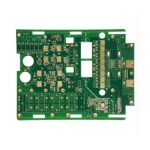
Heavy Copper PCB: Etching and Plating Limits
What Counts as Heavy Copper
Heavy copper usually means a layer of three ounces per square foot or more, which is roughly 105 micrometres, and the term extends to boards with copper an order of magnitude thicker for high current applications. The distinction is not arbitrary: above about two ounces the process changes, because the etching, the plating and the imaging all behave differently and the achievable feature sizes shrink. Above roughly four ounces, the pattern is often built by plating up rather than etching down, and above ten ounces the board is closer to a metal fabrication than to a printed circuit.
How It Is Built
A heavy copper layer is normally produced from a combination of a starting foil and additional plating, or entirely by plating into a resist pattern. In the plating-up method the copper is deposited where the traces will be, using a thick photoresist as a mould, and the surrounding copper is then removed or left as a plane. The advantage is that the trace geometry is defined by the plating rather than by the etchant, which allows thicker traces with more vertical walls and finer spacing than etching alone could achieve. The disadvantage is that it takes a long time in the plating tank and the process has to be controlled closely to keep the thickness uniform.
Etching Heavy Copper
Where the layer is etched, the sidewall angle becomes a serious problem. Etching removes copper in every direction, and in a thick layer the sideways removal is a large fraction of the trace width. A 0.3 mm trace on three-ounce copper can end up with a base width far below the drawn width, and the trapezoid changes the resistance and the thermal behaviour of the trace. The consequence for the design is that the minimum spacing must be large enough for the etchant to clear the gap, and the minimum trace width must be specified as the finished width at the base rather than at the top. Design rules for heavy copper layers are therefore much coarser than for thin ones, and they should be taken from the shop that will build the board.
Plating and Holes
A heavy copper board usually needs heavy plating, because the same current that flows in the traces flows through the vias. A standard 25 micrometre barrel is inadequate for a trace carrying tens of amps, and the barrel becomes the weak point of the circuit both electrically and thermally. Heavy plating takes longer, is more difficult to keep uniform, and reduces the finished hole size by a larger amount, which has to be allowed for in the drill table. The aspect ratio limit also tightens, because a thick board with heavy plating is difficult to plate uniformly along the barrel, and the tendency is to use larger holes and to accept a lower routing density.

Thermal and Current Benefits
The benefits of heavy copper are a larger current capacity for a given width and a much better ability to spread heat. A heavy copper layer can reduce the temperature rise of a hot component significantly, sometimes removing the need for a heatsink or a thermal interface. It also reduces the voltage drop along a power path, which matters in low-voltage high-current designs where a few milliohms of trace resistance is a measurable loss. These benefits are the reason heavy copper appears in motor drives, power supplies, battery management and automotive circuits, and the reason it is often chosen for the thermal improvement even when the current alone would not require it.
Design Rules
Use the shop’s heavy copper design rules rather than the standard ones, and take the minimum width and spacing from them. Specify trace widths as finished dimensions and check the current capacity against the actual copper thickness, not the nominal. Where a heavy copper layer is combined with a fine-line signal layer, keep them separate and expect at least one extra layer to accommodate the separation. Add thermal reliefs only where a joint must be soldered, and use solid connections for the power path. Finally, check the copper balance of the stack, since a heavy layer on one side of the board and a thin one on the other is a warpage risk.
Cost and Lead Time
Heavy copper costs more in material, in plating time, in etching time and in yield, and the shops that can do it are fewer, which lengthens the lead time. The cost rises steeply with thickness, and the achievable feature size falls at the same time, so a design should use the smallest copper weight that satisfies the requirement rather than a weight chosen by habit. Where the requirement is mostly thermal, the alternatives of a thicker copper on one layer, a metal-core substrate or a heatsink should be compared, because heavy copper is not always the cheapest way to move heat out of a component.
Heavy Copper and the Assembly Process
An assembly with heavy copper behaves differently in reflow, because the copper mass acts as a heat sink and the pads take longer to reach temperature. A board with heavy copper planes needs a longer soak and a higher peak to bring the joints at the far end of the plane to soldering temperature, and the profile therefore has to be written around the heaviest copper area rather than the average. Wave and selective soldering are similarly affected: a hole connected to a heavy plane loses heat into the plane faster than the iron or the wave can replace it, which is why thermal reliefs are often retained on heavy copper boards even where the thermal design argues against them. Where the assembly also carries a large component, the effect compounds, and the practical answer is a longer dwell and a confirmation by thermocouple rather than an adjustment to the set point.

FAQ
What is heavy copper? Generally three ounces per square foot or more, roughly 105 micrometres, though the term is used loosely and the process changes above about two ounces.
Why do heavy copper design rules differ? Because etching a thick layer removes a large amount of copper sideways, so the minimum width and spacing are much larger than on a thin layer.
Does heavy copper need heavy plating? Usually yes, because the current flows through the vias as well as along the traces, so the barrel has to carry the same load.
Does heavy copper help thermally? Yes, significantly. It spreads heat much better than a thin layer and can remove the need for a separate heatsink.
Is heavy copper always the best answer for high current? No. Widening traces, using parallel layers, or moving to a metal-core board are sometimes cheaper and simpler.
Conclusion
Heavy copper changes the process rather than merely the thickness, so it should be chosen from the current and thermal requirement and designed to the shop’s own rules. Specify finished widths, allow for heavier plating and larger holes, keep heavy and fine features on separate layers, and check the stack for balance. Process capability is listed under PCB capabilities, the plating and etching steps are described in PCB manufacturing, and the trace sizing belongs to PCB design and layout. Power boards are normally proven through prototype PCB assembly in 2026.