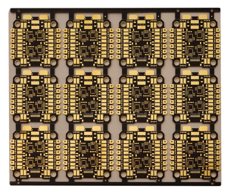
High-Density Multilayer PCB: Why Fabrication Gets Harder
A high-density multilayer PCB is not simply a board with more layers. It is a product where the substrate, the layer-to-layer connection, the copper finish, and the inspection plan all have to be right at the same time, and where a defect in any one of them appears only after the whole stack has been laminated. That is why the difficulty curve rises so steeply as the design shrinks.
Additive and Subtractive Processes
Conductors on a board are formed in one of two ways. The subtractive process starts from a substrate already covered with copper, prints the circuit pattern, and dissolves away the unwanted metal with a chemical etchant. The additive process builds the conductor instead, by plating, evaporating, or otherwise depositing conductive material only where it is wanted. Both are still in use, and the choice correlates with the product: flexible and high-value circuits often use additive processing, while rigid and multilayer boards more commonly use the subtractive route, which explains why multilayer boards dominate by volume.
The substrate underneath decides the rest. The base material sets the mechanical strength, the insulation behavior, and the basic electrical performance, and before flexible films and high-temperature laminates were available, the material was the bottleneck that limited what a board could do. Once films with useful flexibility and laminates with real thermal tolerance arrived, the constraint moved from the material to the process.
Why Density Raises the Difficulty
Multilayer construction exists because it shrinks the board. Stacking several double-sided boards and joining them with plated connections allows the same circuit to occupy a fraction of the area, often several times to more than ten times smaller than an equivalent single-layer layout. That is the benefit. The cost is that the connections between layers become the weakest part of the structure.
Thermal cycling is what exposes them. As the product heats and cools during operation, the board expands and contracts, and a connection that is mechanically marginal will open or become intermittent. The failure is temperature-dependent and often intermittent, which makes it expensive to diagnose. Reducing it is a materials problem: laminates with better dimensional stability and more consistent expansion behavior, together with a process that controls lamination temperature and pressure tightly, are what keep the layer-to-layer joints reliable. The advantages that justify the extra process steps are summarized in multilayer PCB advantages in high-speed designs.

Metal Layers and Surface Finish
The metal on top of the substrate has its own cost structure. Different metals differ widely in price and in behavior, and the choice affects solderability, corrosion resistance, and therefore production cost. Common finishes include tin, tin-lead alloy, and tin-copper alloy, with tin applied at roughly 5 to 15 micrometers and tin-lead alloy at roughly 5 to 25 micrometers. Each is selected for a combination of solderability, shelf life, and process compatibility rather than for electrical performance alone.
Copper exposed to air oxidizes, and oxidized copper solders poorly and can lift. To prevent that, a protective layer is applied to every metal area that will be soldered. The common options are hot air solder leveling, electroless nickel with immersion gold, immersion silver, immersion tin, and organic solderability preservatives. They differ in flatness, in shelf life, in cost, and in how well they tolerate multiple reflow cycles, so the finish should be chosen together with the assembly plan rather than after it. Plating chemistry itself is a process variable with its own failure modes, described in electroplating additives in PCB.
Inspection at Every Stage
Because the process has so many steps, quality control on a multilayer board is distributed rather than final. Each stage gets a first-article check, an end-of-run check, and sampling in between, so that a drift is caught before a whole lot is affected. At drilling, a pin gauge verifies the hole diameter on the first article. At plating, a handheld copper thickness meter checks the deposited copper, and a microsection confirms the copper density in the barrel and the quality of the bond to the inner layers. After plating, edge trimming removes glass fiber, resin, and debris, and a belt sander levels the copper surface and removes nodules and depressions.
At volume, machine vision carries the load. Automated optical inspection conveys panels through a camera system and compares the image against the original artwork to catch open circuits, shorts, and nicks. For multilayer boards, X-ray inspection confirms layer-to-layer registration, which no optical method can see. Each of these answers a different question about the same board, which is why the inspection plan matters as much as the process itself.
Process Control in the Plating and Mask Lines
The chemical steps are where consistency is hardest to hold. Panels pass through a sequence of baths, and each bath has to run at a controlled temperature, for a controlled time, at a controlled rate. The plating chemistry has to be replenished as it is consumed, with pH monitored and adjusted, or the deposit becomes uneven and fine features lose tolerance. Cleanliness belongs to the same discipline: lines handling liquid photoresist should run with particle filtration and panel surface cleaning, because a single dust particle under a fine trace becomes a defect.
Before solder mask is applied, the bare copper goes through pickling, brushing, and micro-etching. The purpose is to remove oxide and copper fines and to roughen the copper surface slightly, which is what gives the mask ink something to grip. After printing, the ink distribution is checked visually, and after curing the thickness is measured with a film gauge. Lamination of a multilayer stack depends on temperature and pressure, and a two-stage press cycle with a longer second stage produces better hardness, flatness, and copper adhesion than a single fast press. The fundamentals of building the stack itself are covered in multilayer PCB prototype requirements.

Verifying the Finished Board
The finished board is verified electrically rather than visually. CAM data drives test fixture software, which generates a program for a fixture of fine probes that contacts the board and checks continuity and isolation on every net. That step is what separates a good panel from a bad one before assembly, and it is also the step whose difficulty grows with density: as pad pitch shrinks, the probes have to be arranged more carefully and the fixture becomes more expensive to build.
The underlying pattern is that density raises the cost of being wrong. A simple board can be inspected by eye and reworked; a high-density multilayer PCB often cannot, because the defect is inside the stack or underneath a component. That is why the inspection and process control budget on these products is high, and why a design that respects the fabricator process window from the beginning is cheaper overall than one that assumes the process will absorb the margin.
FAQ
Why is a multilayer board more prone to intermittent faults? Because the layer-to-layer connections are the mechanically weakest part of the structure, and thermal cycling works on them continuously.
What does X-ray inspection find that optical inspection cannot? Layer-to-layer registration. Optical methods see the surface, while X-ray looks through the stack at the alignment of the inner layers.
Why roughen the copper before applying solder mask? To give the ink mechanical grip. Without the micro-etch, adhesion is poor and the mask lifts during assembly.
Is a two-stage lamination press cycle necessary? It gives better hardness, flatness, and copper adhesion than a single fast press, which matters more as layer count and density rise.