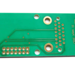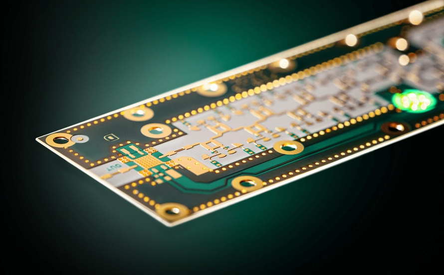
High-Frequency PCB Design: PCB Design, PCB Manufacturing, Signal Integrity & High-Speed Layout Guide
As electronic products continue to become faster, smaller, and more interconnected, the demand for high-frequency and high-speed electronic systems is increasing rapidly. Telecommunications equipment, aerospace systems, medical devices, high-performance computing platforms, automotive electronics, radar systems, and wireless communication products all depend on reliable high-speed signal transmission.
As operating frequencies and data rates increase, conventional PCB layout techniques may no longer provide sufficient signal integrity. Designers must consider controlled impedance, dielectric properties, transmission-line geometry, return paths, crosstalk, electromagnetic interference (EMI), thermal management, and manufacturing tolerances from the earliest stages of development.
A successful High-Frequency PCB Design therefore requires much more than simply routing traces with smaller geometries. The electrical behavior of the entire interconnect—including the PCB material, trace structure, reference plane, vias, connectors, and return path—must be considered as part of the signal-transmission system.
This guide explains the major principles of high-frequency PCB Design and PCB Manufacturing, providing practical guidance for engineers working on high-speed and RF-related circuit boards.
What Is High-Frequency PCB Design?
High-frequency PCB design refers to designing printed circuit boards capable of transmitting high-frequency signals while maintaining signal integrity, predictable impedance, and acceptable electromagnetic performance.
The term “high frequency” is often used for signals above approximately 1 GHz, although there is no single frequency threshold that universally defines a high-frequency PCB. In practice, a PCB can require high-frequency design techniques at lower frequencies when signal rise time is sufficiently fast or interconnect dimensions become electrically significant.
At high frequencies, PCB traces behave increasingly like transmission lines rather than simple electrical connections.
Poor layout can result in:
- Signal reflection
- Insertion loss
- Return loss
- Crosstalk
- Electromagnetic interference
- Ground noise
- Timing distortion
- Impedance discontinuities
- Excessive attenuation
Therefore, maintaining Signal Integrity is one of the most important objectives of high-frequency PCB design.
Key Concepts in High-Frequency PCB Design
1. Signal Integrity
Signal integrity describes how accurately an electrical signal maintains its intended voltage, timing, waveform, and noise characteristics as it travels through an interconnect.
Poor signal integrity can cause:
- Data corruption
- Increased bit-error rates
- Timing failures
- Reduced system performance
- Intermittent operation
- Communication failures
Several factors influence signal integrity, including trace geometry, dielectric properties, impedance, via structures, connectors, return paths, and power-distribution characteristics.
To improve signal integrity, designers should minimize unnecessary discontinuities and control reflection, loss, and electromagnetic coupling.
2. Controlled Impedance
Controlled impedance is one of the most important principles in high-frequency PCB design.
When a high-speed signal travels through a PCB trace, the trace and its reference structure form a transmission line with a characteristic impedance.
If the impedance changes abruptly, part of the signal can be reflected toward the source.
Impedance discontinuities can occur because of:
- Changes in trace width
- Changes in dielectric thickness
- Layer transitions
- Via structures
- Connectors
- Pads
- Stubs
- Plane discontinuities
- Improper stackup construction
Common controlled-impedance values include 50 Ω for many single-ended RF interfaces and 90 Ω or 100 Ω for certain differential interfaces, but the correct target must be determined by the system specification and interface standard.
3. Dielectric Materials
The PCB dielectric material plays a major role in high-frequency performance.
Two important material properties are:
- Dielectric constant (Dk)
- Dissipation factor (Df)
A stable Dk helps maintain predictable impedance and propagation characteristics.
A lower Df generally means lower dielectric loss, which can be important for high-frequency and long-channel applications.
Material selection should also consider:
- Dk stability over frequency
- Df stability over frequency
- Temperature dependence
- Moisture absorption
- CTE
- Copper roughness
- Mechanical reliability
- Availability
- Manufacturing compatibility
Standard FR-4 can be suitable for many high-speed designs, but specialized low-loss laminates may be preferred when signal loss, Dk stability, or RF performance becomes a critical requirement.
4. Return Path
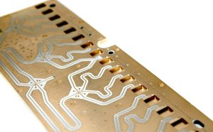
Every high-frequency signal requires a corresponding return-current path.
The return current tends to follow the path of lowest impedance, which at high frequencies is strongly influenced by the reference plane directly adjacent to the signal trace.
A discontinuous return path can cause:
- Increased loop inductance
- Impedance discontinuity
- Increased radiation
- Greater crosstalk
- Higher EMI
Therefore, high-speed traces should generally be routed over a continuous reference plane.
Avoid routing critical signals across gaps or splits in the reference plane unless the return path is intentionally designed and controlled.
Basic High-Frequency PCB Design Guidelines
1. Material Selection
Selecting the appropriate PCB laminate is one of the first decisions in high-frequency PCB development.
Low and Stable Dk
The dielectric constant affects signal propagation velocity and transmission-line impedance.
For controlled-impedance applications, designers need a material with predictable Dk across the relevant frequency and temperature range.
Low Df
A lower dissipation factor generally helps reduce dielectric loss, particularly as frequency and transmission distance increase.
However, Dk and Df should not be evaluated in isolation. Material selection must also consider PCB fabrication capability, reliability, cost, layer count, copper roughness, and the final operating environment.
2. Controlled-Impedance Design
Controlled impedance requires coordination between the PCB designer and manufacturer.
Important parameters include:
- Trace width
- Trace thickness
- Dielectric thickness
- Copper roughness
- Dk
- Reference-plane spacing
- Layer stackup
Calculate Trace Impedance
Impedance should be calculated using an appropriate field solver or stackup-design tool rather than relying solely on simple formulas.
For production designs, the final impedance target should be based on the actual material system and fabrication process.
Maintain Impedance Consistency
A controlled-impedance trace should maintain consistent geometry throughout its routing path.
Abrupt changes in width, reference-plane distance, or layer structure can introduce discontinuities.
Differential Pairs
Differential interfaces should be routed as properly matched differential pairs.
Important considerations include:
- Differential impedance
- Pair spacing
- Trace-width matching
- Length matching where required
- Reference-plane continuity
- Via symmetry
- Avoidance of unnecessary stubs
Length matching should be based on the interface’s timing budget rather than applied excessively to every high-speed signal.
3. Transmission-Line Design
At high frequencies, PCB traces should be treated as transmission lines.
Two common PCB transmission-line structures are microstrip and stripline.
Microstrip
A microstrip consists of a signal conductor on an outer PCB layer with a reference plane separated by dielectric material.
Microstrip structures are widely used in RF and microwave circuits because they provide accessible routing and can be convenient for component connections.
Stripline
A stripline places the signal conductor between reference planes within the PCB stackup.
Stripline structures can provide strong electromagnetic containment and a well-controlled transmission environment.
The choice between microstrip and stripline depends on:
- Required impedance
- Layer count
- EMI requirements
- Routing density
- Manufacturing capability
- Thermal requirements
- Connector transitions
- Overall system architecture
4. Ground Planes and Return Paths
A continuous reference plane is fundamental to reliable high-frequency PCB design.
The reference plane provides a predictable return-current path and helps reduce loop area.
Designers should avoid unnecessary plane splits underneath critical high-speed traces.
Ground Stitching
Ground stitching vias can connect reference planes across PCB layers and help maintain a low-impedance reference structure.
They can be especially useful around:
- RF sections
- Board edges
- Shielding structures
- Connector transitions
- Layer transitions
- High-speed interfaces
However, stitching vias should be positioned according to the electrical requirements of the design rather than simply adding as many vias as possible.
5. Crosstalk Reduction
Crosstalk occurs when energy from one signal couples into a nearby signal.
At high frequencies, both capacitive and inductive coupling can become significant.
Increase Trace Spacing
Increasing the spacing between sensitive traces can reduce electromagnetic coupling.
A common practical approach is to maintain greater separation between high-speed signal traces and particularly sensitive analog or RF lines.
The appropriate spacing depends on:
- Trace geometry
- Dielectric thickness
- Frequency
- Routing layer
- Reference-plane configuration
- Parallel routing length
Minimize Parallel Routing
Long parallel runs between aggressor and victim traces can increase crosstalk.
Where practical, designers should reduce unnecessary parallel routing.
Orthogonal Routing
When adjacent signal layers must cross, routing directions can sometimes be arranged approximately orthogonally to reduce broadside coupling.
However, maintaining a continuous reference plane and controlling stackup geometry is generally more important than simply applying a 90-degree routing rule.
6. Thermal Management
Thermal management is another important aspect of high-frequency PCB design.
High-speed processors, RF amplifiers, power-management devices, transceivers, and other active components can generate significant heat.
Excessive temperature can change electrical characteristics and negatively affect reliability.
Heat Sinks
Heat sinks can be used for components with significant thermal loads.
The heat-transfer path should be designed from the semiconductor junction through the package and PCB into the heat-spreading or heat-sinking structure.
Thermal Vias
Thermal vias can transfer heat from component pads into internal or bottom copper structures.
For high-power devices, an array of thermal vias can help distribute heat across a larger copper area.
Thermal Interface Materials
Thermal pads, thermal interface materials, or thermal compounds can be used to reduce thermal resistance between the PCB assembly and a heat sink or chassis.
Thermal design should be evaluated together with electrical requirements because temperature can affect material properties, component performance, and long-term reliability.
7. Prototype Development and Testing
Prototype development is essential for validating high-frequency PCB performance before mass production.
A prototype allows engineers to identify problems related to:
- Signal integrity
- Impedance
- Crosstalk
- EMI
- Thermal performance
- Component selection
- Manufacturing tolerances
Signal Integrity Testing
Signal integrity testing can include measurements of:
- Rise and fall time
- Overshoot
- Undershoot
- Jitter
- Eye diagrams
- Insertion loss
- Return loss
The exact measurements depend on the interface and system requirements.
Impedance Testing
Time-domain reflectometry (TDR) can be used to identify impedance discontinuities along a transmission path.
TDR measurements can help locate problems associated with:
- Trace transitions
- Vias
- Connectors
- Pads
- Stackup changes
RF Testing
For RF applications, a vector network analyzer (VNA) can be used to characterize parameters such as insertion loss and return loss.
Testing should be performed using appropriate fixtures, calibration methods, and measurement procedures.
Advanced High-Frequency PCB Design Techniques
1. Use Electromagnetic Simulation
Electromagnetic simulation can help engineers analyze high-frequency behavior before physical fabrication.
Simulation can be used to investigate:
- Signal propagation
- Reflection
- Crosstalk
- Electromagnetic coupling
- Antenna effects
- Via transitions
- Connector transitions
- Transmission-line behavior
Simulation is particularly valuable when the design contains complex stackups, high-speed interfaces, RF structures, or tight impedance requirements.
By identifying problems before fabrication, engineers can reduce prototype iterations and development costs.
2. Perform Signal Integrity Analysis
Signal integrity analysis should be integrated into the design process rather than performed only after prototype fabrication.
Tools and measurement equipment such as TDRs, oscilloscopes, and VNAs can help engineers evaluate signal behavior.
A comprehensive analysis can identify:
- Impedance mismatch
- Signal reflection
- Attenuation
- Crosstalk
- Timing problems
- Excessive loss
- Discontinuities
The results can then be used to optimize trace geometry, stackup, termination, vias, connectors, and component placement.
3. Use Differential Signaling
Differential signaling is widely used in high-speed digital and communication systems because it can improve immunity to common-mode interference when implemented correctly.
Examples of differential interfaces include various high-speed serial buses and RF or communication architectures.
Effective differential-pair design requires attention to:
- Differential impedance
- Pair geometry
- Reference-plane continuity
- Pair symmetry
- Via transitions
- Skew
- Connector transitions
- Common-mode behavior
Simply routing two traces next to each other does not automatically create a well-controlled differential pair.
4. Optimize Via Design
Vias can introduce discontinuities into high-frequency transmission lines.
A via transition can introduce:
- Parasitic capacitance
- Parasitic inductance
- Impedance discontinuity
- Signal reflection
- Resonance
- Additional insertion loss
Therefore, via structures should be carefully optimized.
Blind and Buried Vias
Blind and buried vias can reduce unnecessary signal transitions through unused PCB layers.
They can also help reduce via stubs in high-density multilayer designs.
However, they increase manufacturing complexity and cost, so they should be used when their electrical or routing benefits justify the additional PCB Manufacturing requirements.
Backdrilling
Backdrilling removes unused portions of through-hole vias to reduce long via stubs.
This technique can be particularly useful in high-speed multilayer PCBs where via-stub resonance could negatively affect signal integrity.
The required backdrill depth and remaining stub length should be controlled according to the signal frequency and stackup.
High-Frequency PCB Manufacturing Considerations
High-frequency performance depends not only on PCB layout but also on fabrication consistency.
During PCB Manufacturing, several parameters must be carefully controlled.
Material and Stackup Control
The actual dielectric thickness and Dk influence controlled impedance.
Therefore, the PCB manufacturer should provide a stackup based on the actual material system rather than relying only on nominal CAD values.
Copper Roughness
At high frequencies, conductor loss can be affected by copper surface roughness because of the skin effect.
For demanding applications, smoother copper may help reduce conductor loss.
Etching Accuracy
Trace-width variation can directly affect controlled impedance.
Therefore, fabrication tolerances should be incorporated into the design and impedance-control strategy.
Registration Accuracy
Multilayer registration affects:
- Differential-pair symmetry
- Via transitions
- Pad alignment
- Controlled impedance
- Fine-pitch structures
High-density and high-frequency designs require appropriate manufacturing tolerances.
Impedance Testing
Production impedance testing can verify whether manufactured transmission lines meet the specified target.
A good PCB Manufacturing process should therefore connect design specifications with fabrication tolerances and measurement requirements.
Common High-Frequency PCB Design Mistakes
Several common mistakes can compromise high-frequency PCB performance.
1. Treating High-Speed Traces Like Ordinary Wires
At sufficiently high frequencies or fast edge rates, interconnects behave as transmission lines. Ignoring this behavior can lead to reflection and timing problems.
2. Ignoring the Return Path
A signal trace without a predictable return path can produce excessive loop area and electromagnetic radiation.
3. Using an Uncontrolled Stackup
Changing dielectric thickness or material properties can change trace impedance.
4. Excessive Via Stubs
Long via stubs can behave as resonant structures and degrade high-speed signals.
5. Routing Across Plane Splits
Crossing gaps in the reference plane can force return current to take a longer path and create impedance discontinuities.
6. Excessive Parallel Routing
Long parallel traces can increase capacitive and inductive coupling.
7. Choosing Materials Only by Cost
A low-cost material may be appropriate for many applications, but demanding high-frequency designs may require tighter Dk/Df control and lower-loss materials.
8. Ignoring Manufacturing Tolerances
A simulation based on ideal geometry does not guarantee that the manufactured PCB will have exactly the same electrical characteristics.
How to Improve High-Frequency PCB Design
A practical development workflow can include the following steps:
- Define the frequency, data rate, rise/fall time, and electrical requirements.
- Identify all controlled-impedance interfaces.
- Select the appropriate PCB material.
- Develop the multilayer stackup.
- Define impedance targets and manufacturing tolerances.
- Establish continuous reference planes.
- Design high-speed transmission lines.
- Optimize differential pairs.
- Minimize unnecessary vias and via stubs.
- Control crosstalk through spacing and routing strategy.
- Optimize connectors and layer transitions.
- Perform signal integrity and electromagnetic simulations.
- Conduct DFM and impedance reviews with the PCB manufacturer.
- Build prototypes.
- Perform TDR, VNA, oscilloscope, thermal, and EMI testing as appropriate.
- Correct design problems before mass production.
This approach allows engineers to identify electrical and manufacturing risks early instead of discovering them after large-scale production.
High-Frequency PCB Design and Manufacturing with Kingda
For demanding high-frequency and high-speed applications, cooperation between the PCB design team and manufacturing partner is critical.
Kingda can support PCB fabrication and PCBA development for applications requiring controlled manufacturing processes and specialized PCB structures.
Depending on project requirements, a manufacturing partner can assist with:
- Material selection
- Stackup development
- Controlled-impedance PCB fabrication
- High-density multilayer PCB manufacturing
- HDI structures
- Backdrilling
- DFM analysis
- Prototype fabrication
- SMT assembly
- AOI inspection
- X-ray inspection
- Electrical testing
- Functional validation
Early manufacturing involvement allows designers to evaluate material availability, trace geometry, layer structures, via technologies, impedance tolerances, and production limitations before the design is released.
This is especially important for high-frequency boards because a small difference between the simulated design and the manufactured structure can affect real-world signal performance.
Conclusion
High-frequency PCB design is a multidisciplinary engineering process that requires careful control of electrical, material, mechanical, thermal, and manufacturing parameters.
The most important considerations include Signal Integrity, controlled impedance, dielectric material selection, transmission-line geometry, continuous return paths, crosstalk reduction, thermal management, differential signaling, via optimization, electromagnetic simulation, and prototype testing.
As data rates and operating frequencies continue to increase, traditional PCB layout methods are no longer sufficient for many demanding applications. Engineers must consider the complete signal path from the transmitter to the receiver, including traces, vias, connectors, reference planes, and return-current paths.
At the same time, successful PCB Manufacturing requires accurate material selection, stackup control, trace fabrication, multilayer registration, impedance verification, and manufacturing-tolerance management.
By integrating PCB Design and PCB Manufacturing considerations from the beginning, engineers can build high-frequency circuit boards with better signal integrity, lower loss, improved EMI performance, and greater long-term reliability.
Article Summary
High-frequency PCB design focuses on maintaining reliable signal transmission as operating frequency and data rates increase. Controlled impedance, low-loss materials, continuous reference planes, optimized transmission lines, proper return paths, differential routing, crosstalk reduction, and carefully designed vias are essential for high-frequency performance.
Advanced methods such as electromagnetic simulation, signal integrity analysis, TDR testing, VNA measurements, blind and buried vias, and backdrilling can further improve high-speed PCB performance.
However, high-frequency performance cannot be separated from manufacturing quality. Material tolerances, dielectric thickness, copper roughness, trace-width accuracy, multilayer registration, and impedance control all influence the final PCB.
Therefore, the best approach is to treat PCB Design and PCB Manufacturing as an integrated engineering process rather than separate stages.
SEO Keywords
High-Frequency PCB, PCB Design, PCB Manufacturing, High-Frequency PCB Design, High-Speed PCB, Signal Integrity, Controlled Impedance PCB, RF PCB, High-Speed PCB Design, PCB Signal Integrity
Google TDK
SEO Title:
High-Frequency PCB Design: PCB Design, PCB Manufacturing & Signal Integrity
Meta Description:
Learn high-frequency PCB design principles, including controlled impedance, PCB materials, transmission lines, return paths, crosstalk, vias, EMI, signal integrity, and PCB manufacturing.
Meta Keywords:
High-Frequency PCB, PCB Design, PCB Manufacturing, High-Frequency PCB Design, High-Speed PCB, Signal Integrity, Controlled Impedance PCB, RF PCB, High-Speed PCB Design, PCB Signal Integrity