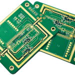
High-Frequency PCB Manufacturing Key Process Requirements
High-frequency boards fail for reasons that rarely appear on the drawing. A dielectric layer presses a few microns thin, a drill bit wears past its limit, or an etch line drifts wide, and the impedance moves with it. The electrical target set during design only survives if each fabrication step holds its own window. This review walks through the process stages in order, from incoming laminate to final test. It focuses on what changes the result and what a buyer should verify before release.
Signal loss and impedance both depend on physical geometry. Dielectric thickness, copper roughness, trace width, and layer registration all shift the electrical behavior of a transmission line. A conventional board tolerates small drift because the design margin absorbs it. A high-frequency design has far less room, so the same drift becomes a yield problem. Every stage below therefore needs a defined limit, a recorded measurement, and a person who checks it. That discipline starts with the material itself.
Material Selection and Storage
Low-loss laminates form the base of any high-frequency stackup. PTFE systems, ceramic-filled materials, and similar low-loss dielectrics behave differently from standard FR-4, and each has its own process window. The laminate, prepreg, and copper foil must be matched as a set so the multilayer structure stays consistent. Copper foil choice matters as much as the dielectric. At high frequencies the skin effect pushes current toward the surface, so a low-profile foil reduces conductor loss.
Buyers should confirm the exact foil type on the stackup drawing rather than accept a generic note. A vague entry such as low-profile copper leaves the fabricator free to substitute a standard foil when stock runs short. That substitution changes conductor loss without changing any other number on the drawing, so the board still passes dimensional checks. The stackup should name the foil class, the dielectric grade, and the prepreg type. Each of those three items should also appear on the incoming inspection record.
Incoming material needs inspection before it reaches lamination. Batch-to-batch variation in dielectric constant or thickness will move impedance even when every machine setting is correct. Storage conditions deserve the same attention. Controlled temperature and humidity limit moisture absorption, oxidation, and dimensional change. Prepreg that absorbs moisture can trap volatiles during pressing and leave voids in the bond line. A simple rule helps here: verify the material certificate, check the batch, and confirm the storage record. These steps cost little and remove a common source of drift.
Lamination and Dielectric Control
Lamination sets the dielectric thickness that the impedance calculation assumed. Standard press recipes do not transfer directly to high-frequency materials. Temperature, pressure, heating rate, hold time, and cooling profile should be developed for the specific laminate and prepreg combination. Low pressure can leave voids or weak bonds between layers. Excessive heat or a poor cycle can change the material’s electrical and mechanical properties. The press cycle should be documented and repeated, not adjusted by feel on each lot.
Resin flow is the quiet variable in this step. Too little flow leaves dry spots and weak bond lines, while too much flow starves the edges and thins the dielectric under heavy copper. Both outcomes change the local dielectric thickness, and neither shows up until a coupon is measured. A shop should record the flow window for each prepreg style and check panel edges after cure. Buyers can ask how the press operator confirms that flow stayed inside that window on the last lot.
Layer registration matters just as much as thickness. Any offset between a signal layer and its reference plane changes the local dielectric geometry and shifts impedance. Precise lay-up and alignment procedures reduce that risk. Vacuum lamination and controlled cooling can improve bond consistency and limit warpage on demanding stackups. Buyers should ask for the lamination window and the registration tolerance in writing. They should also ask how the shop verifies dielectric thickness after cure, because a coupon measurement tells more than a press setting ever will.

Drilling and Hole-Wall Treatment
High-frequency laminates vary widely in mechanical behavior. Some are soft and prone to burrs or hole deformation. Ceramic-filled grades are harder and wear tools faster. Drilling parameters should follow the material, not a default recipe. Feed rate, spindle speed, drill type, and stack height all affect hole quality. On soft materials, poor conditions can smear the hole wall or change the diameter. On hard filled materials, worn tools drift in diameter and position, so tool-life management and scheduled replacement are essential.
Small holes and microvias may need laser drilling for better dimensional control. After drilling, desmear and hole-wall preparation remove resin residue and prepare the surface for plating. This step matters more when vias sit inside high-frequency transmission structures, because a rough or contaminated wall adds loss and can disturb the return path. A buyer should confirm the desmear method and the plating thickness target. Both belong in the process record, and both should be checked on the first article before the lot proceeds.
Drill wander deserves a separate check on thin high-frequency panels. A bit that deflects at entry shifts the hole center, and the shift grows with stack height and with softer dielectric. The result is an annular ring that looks acceptable on one side and thin on the other. Cross-sections taken from the outer edges of the panel reveal this faster than center samples. Buyers should ask where the samples were cut, because a center-only check can hide the worst registration on the lot.
Imaging and Etching Accuracy
Circuit formation fixes the geometry of every transmission line. Trace width, spacing, copper thickness, and edge profile all feed into impedance. Laser direct imaging can improve pattern accuracy and registration on fine features compared with conventional exposure. The etch step then decides whether the drawn width survives. Excessive lateral etching narrows traces and changes the intended geometry. Uneven edges add conductor loss at high frequency, and the effect grows as the trace narrows.
Shops should control etch compensation, side etch, and line-edge quality as named parameters. The finished conductor geometry must stay inside the tolerance used for the impedance calculation. If the etcher cannot hold that tolerance, the stackup needs review before production, not after. Buyers can request cross-section data from a test coupon to confirm what the process actually produced. That measurement, taken from a real panel, is stronger evidence than a specification sheet. It also gives the engineer a baseline for the next order.
Copper thickness interacts with etch in a way that surprises new buyers. Heavier copper needs longer etch time, and longer etch time widens side etch on every trace. A design that specifies heavy copper for current capacity may therefore lose trace width control on the same layer. The fabricator should flag that conflict during the DFM review rather than compensate silently. Buyers should ask whether the quoted trace width is the drawn width or the finished width, because the two differ by the etch allowance.

Surface Finish and Profiling
Surface finish affects both electrical behavior and assembly yield. A flat, uniform finish is generally preferred for high-frequency boards, especially where fine-pitch parts or high-speed interconnects are used. ENIG, immersion silver, ENEPIG, and OSP each bring tradeoffs in flatness, cost, and shelf life. The coating must stay uniform in thickness and free of oxidation, contamination, and peeling. The right choice depends on the assembly process, the reliability target, and the service environment, so it should be agreed early rather than left to the fabricator.
Routing and profiling come last and can still damage a good panel. High-frequency laminates are often more sensitive to mechanical stress and dimensional deformation. Sharp tools and suitable cutting parameters reduce chipping, delamination, and burrs. Final inspection should cover dimensions, edge quality, warpage, cleanliness, layer integrity, and hole quality. Small physical defects matter more here because signal performance tracks the physical path so closely. A nick at the board edge is cosmetic on a low-speed design and a real risk on a high-frequency one.
Impedance Test and Verification
Inspection should prove that the physical board matches the electrical requirement. For controlled-impedance designs, coupons and TDR testing verify actual values against the specified tolerance for single-ended and differential structures. The parameters under watch include trace width, copper thickness, dielectric thickness, dielectric constant, reference-plane spacing, and copper roughness. Each one can move the result, so each one needs a recorded value. Testing without a record leaves the next lot guessing.
Additional checks usually include automated optical inspection, dimensional measurement, cross-section analysis, and electrical test. Functional verification belongs to the assembly stage, where PCBA testing confirms the finished unit under power. A structured quality management system ties these records together so a repeat order starts from data rather than memory. Buyers should ask which parameters are measured, on what sample size, and where the results are stored. Clear answers show that the process is controlled in practice, not only described in a brochure.
Coordinating Design and Fabrication
Impedance cannot be controlled by layout alone. The final value depends on the interaction between design geometry, material properties, stackup construction, and manufacturing tolerance. A small change in trace width, dielectric thickness, or reference distance shifts the result. Engineers should therefore agree the stackup with the fabricator before routing is frozen. Manufacturer feedback can confirm that the chosen materials, prepreg combinations, and tolerances fit real production capability. That conversation is cheaper than a respin.
The same logic carries into assembly. When the board moves to SMT PCB assembly, the finish, flatness, and warpage from fabrication affect placement yield. Early samples built through rapid PCBA prototyping reveal pad and process issues while changes are still inexpensive. For volume builds, a partner that handles PCB assembly under one roof keeps fabrication and assembly data aligned. The takeaway for buyers is simple. Ask for the stackup, the process windows, and the measurement records before you place the order, and confirm who owns each tolerance.