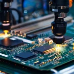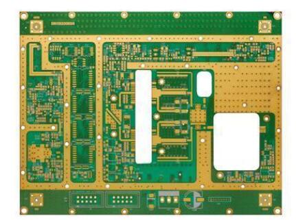
As electronic systems continue to operate at higher frequencies and data rates, the demand for advanced High-Frequency PCB technology is increasing rapidly. Communication systems, radar, automotive electronics, satellite equipment, wireless networks, and other RF applications increasingly require circuit boards with stable electrical performance, low signal loss, precise impedance control, and excellent dimensional stability.
A High-Frequency Circuit Board is designed to support the transmission of high-frequency electrical signals. Although there is no single universal frequency threshold that defines a high-frequency PCB, the term is commonly used for circuits operating in the GHz range, particularly in RF and microwave applications.
Microwave applications can extend from several GHz into the millimeter-wave range, where even small variations in material properties or conductor geometry can significantly affect signal performance.
Compared with conventional FR-4 circuit boards, High-Frequency PCB fabrication requires greater attention to dielectric properties, copper surface roughness, trace geometry, drilling, plating, lamination, and material-specific processing.
1. What Is a High-Frequency PCB?
A High-Frequency PCB is a circuit board specifically designed and manufactured for high-frequency signal transmission. It typically uses specialized dielectric materials with controlled electrical properties rather than relying exclusively on conventional FR-4 materials.
The performance of a high-frequency circuit is strongly influenced by the relationship between frequency, dielectric properties, conductor geometry, and transmission-line structure.
Important electrical parameters include:
- Dielectric constant (Dk)
- Dissipation factor (Df)
- Dielectric thickness
- Copper thickness
- Copper surface roughness
- Characteristic impedance
- Insertion loss
- Signal attenuation
- Thermal stability
- Dimensional stability
As operating frequency increases, material selection becomes increasingly important. A substrate with a stable Dk and low Df can help reduce dielectric loss and maintain more predictable signal behavior.
For RF and microwave designs, PCB performance should therefore be evaluated as a complete system rather than based on a single material specification.
2. Applications of High-Frequency PCBs
The demand for RF PCB technology continues to grow as wireless and high-speed electronic systems become more advanced.
Typical applications include:
Mobile and Wireless Communication
High-Frequency PCB technology is widely used in wireless communication equipment, RF modules, base-station systems, antennas, power amplifiers, and low-noise amplifiers.
RF Passive Components
High-frequency circuit boards are also used for RF passive circuits such as:
- Power dividers
- Couplers
- Duplexers
- Filters
- Matching networks
- Antenna feed networks
- Impedance transformers
The dimensional accuracy and dielectric properties of the PCB can directly affect the electrical performance of these structures.
Automotive Radar
Automotive radar systems increasingly operate at high frequencies, particularly around the 24 GHz and 77–81 GHz ranges.
At these frequencies, PCB material selection, trace geometry, surface roughness, dielectric thickness, and manufacturing tolerances can have a significant impact on radar performance.
Satellite and Aerospace Electronics
Satellite communication, navigation systems, radar, avionics, and aerospace communication equipment often require stable electrical performance across demanding temperature and environmental conditions.
High-frequency materials are selected according to electrical loss, thermal stability, dimensional stability, and reliability requirements.
Wireless and Microwave Equipment
A Microwave PCB can also be used in wireless transceivers, microwave modules, test equipment, antennas, and other RF systems where controlled high-frequency signal transmission is required.
3. High-Frequency PCB Material Classification
Material selection is one of the most important aspects of High-Frequency PCB Manufacturing.
Different applications require different combinations of electrical, thermal, mechanical, and processing characteristics.
High-frequency PCB materials can broadly be divided into several categories.
3.1 Ceramic-Filled Hydrocarbon or Thermoset Materials
Some high-frequency laminates use ceramic fillers combined with hydrocarbon-based or thermoset resin systems.
Examples include materials such as:
- Rogers RO4350B
- Rogers RO4003C
- Arlon high-frequency laminate families
- Taconic high-frequency materials
These materials can provide low dielectric loss and controlled electrical characteristics while generally being easier to process than traditional PTFE materials.
Their manufacturing processes can be relatively similar to conventional epoxy/glass PCB fabrication, but special attention may be required because some high-frequency laminates are more brittle.
Drilling and routing tool life can also differ from standard FR-4 production.
3.2 PTFE-Based High-Frequency Materials
PTFE PCB materials are widely used in demanding RF and microwave applications because PTFE-based dielectric systems can provide very low dielectric loss and stable high-frequency performance.
Common PTFE-based material families include various products from specialized RF laminate manufacturers.
However, PTFE substrates can be more difficult to process than conventional FR-4 because of their mechanical characteristics and low surface energy.
Therefore, PCB Materials selection must consider both electrical performance and manufacturing compatibility.
4. PTFE PCB Processing Requirements
Manufacturing a PTFE PCB requires process parameters specifically adapted to the material.
Cutting
PTFE-based laminates should be handled carefully during cutting and transportation.
A protective film or appropriate protective material may be used to reduce the risk of:
- Scratches
- Surface dents
- Creases
- Contamination
- Mechanical damage
The cutting process should maintain board flatness and dimensional stability.
Drilling
Drilling is one of the most important manufacturing steps for PTFE-based boards.
Compared with conventional FR-4, PTFE materials can require different drill parameters and hole-preparation methods.
Important considerations include:
- Drill geometry
- Spindle speed
- Feed rate
- Retract speed
- Chip load
- Drill wear
- Hole-wall quality
- Burr control
Fresh or properly maintained drills should be used for precision applications. Drill parameters should be optimized according to hole diameter, material construction, board thickness, and stack-up.
After drilling, holes should be thoroughly cleaned to remove debris and particles.
Hole-Wall Treatment
PTFE has a relatively low surface energy, which can make conventional chemical metallization more challenging.
Therefore, specialized surface activation may be required before copper deposition.
Depending on the material system and manufacturing process, methods such as plasma treatment or chemical activation can improve the surface condition and promote reliable copper adhesion.
The selected process should be validated for the specific laminate construction rather than applied as a universal recipe.
5. PTH Copper Plating
For High-Frequency PCB designs using plated through-holes, reliable hole metallization is essential.
After drilling and hole preparation, the PCB undergoes a sequence of cleaning, activation, electroless copper deposition, and electroplating processes.
Process control should focus on:
- Hole-wall cleanliness
- Surface activation
- Copper adhesion
- Copper thickness
- Plating uniformity
- Via and PTH reliability
A controlled copper-plating process ensures that the finished holes can provide stable electrical connections and sufficient mechanical reliability.
For specialized microwave materials, the surface preparation and metallization sequence may need to be adjusted to achieve reliable copper adhesion.
6. Dry Film and Image Transfer
The circuit pattern must be transferred accurately onto the PCB surface before etching.
For fine-line High-Frequency PCB Manufacturing, dry-film selection, lamination, exposure, development, and registration must be carefully controlled.
Important factors include:
- Dry-film thickness
- Surface cleanliness
- Lamination temperature
- Exposure energy
- Artwork resolution
- Registration accuracy
- Developing conditions
Poor image transfer can lead to line-width variation, open circuits, shorts, or impedance deviations.
Therefore, image-transfer accuracy is directly related to the final electrical performance of the PCB.
7. PCB Etching
Etching determines the final geometry of the copper circuit.
For high-frequency boards, trace geometry is particularly important because even relatively small variations in trace width or spacing can influence characteristic impedance.
During PCB Manufacturing, etching parameters should be carefully controlled, including:
- Etchant concentration
- Etchant temperature
- Spray pressure
- Conveyor speed
- Copper loading
- Etch compensation
The objective is to maintain clean trace edges with minimal undercut, over-etching, burrs, or notches.
After etching, the circuit should be inspected to confirm that line width and spacing remain within the specified tolerances.
8. Solder Mask Processing
Applying solder mask to high-frequency materials can require different surface preparation compared with conventional FR-4.
The surface should be properly cleaned before solder mask application. Mechanical treatment should be selected carefully because aggressive abrasion can damage specialized dielectric materials.
A typical solder mask process may include:
- Surface cleaning
- Solder mask coating
- Pre-curing
- Exposure
- Development
- Final curing
- Visual inspection
The curing profile must be compatible with the substrate and solder mask system.
Excessive thermal exposure can potentially cause dimensional or material-related issues, especially for multilayer structures containing different dielectric systems.
9. Copper Surface and Lamination Protection
During processing, the copper surface of a High-Frequency Circuit Board should be protected from scratches, contamination, and mechanical damage.
When boards are stacked or laminated, suitable separator materials can be used to prevent copper-to-copper contact and surface damage.
Special care should be taken during:
- Panel stacking
- Lamination
- Routing
- Board handling
- Inspection
- Packaging
For high-frequency applications, copper surface condition can influence conductor loss. Therefore, protecting the copper surface is not simply an appearance requirement—it can also contribute to consistent RF performance.
10. NPTH and PTH Processing Flows
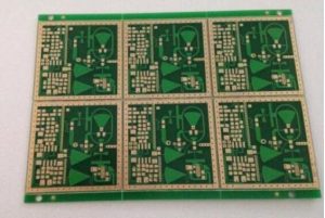
The exact manufacturing process depends on whether the design requires non-plated through-holes (NPTH) or plated through-holes (PTH).
Typical NPTH PTFE PCB Process
A general process flow may include:
Cutting → Drilling → Dry Film → Inspection → Etching → Etch Inspection → Solder Mask → Silkscreen → Surface Finish → Routing/Forming → Electrical Testing → Final Inspection → Packaging → Shipment
The exact sequence may vary according to the board structure and surface-finish requirements.
Typical PTH PTFE PCB Process
A typical PTH process may include:
Cutting → Drilling → Hole Treatment/Activation → Electroless Copper → Electroplating → Dry Film → Image Transfer → Etching → Etch Inspection → Solder Mask → Silkscreen → Surface Finish → Routing/Forming → Electrical Testing → Final Inspection → Packaging → Shipment
Additional processes may be introduced depending on the board design, via structure, layer count, and customer specifications.
11. Quality Control for High-Frequency PCB Manufacturing
Because RF and microwave circuits can be highly sensitive to manufacturing variation, quality control must cover both electrical and physical parameters.
Kingda’s manufacturing process can incorporate inspection and control of:
- Material specifications
- Board thickness
- Dielectric thickness
- Copper thickness
- Trace width and spacing
- Hole diameter
- Hole-wall quality
- Layer registration
- Impedance
- Surface finish
- Solder mask quality
- Board dimensions
- Electrical continuity and isolation
For critical high-frequency products, impedance testing and material verification should be incorporated into the quality-control plan.
The use of test coupons can also help verify that production parameters remain within the required electrical and dimensional tolerances.
12. Design Considerations for High-Frequency PCBs
Good PCB Materials alone cannot guarantee high-frequency performance. The PCB layout and manufacturing process must work together.
Designers should consider:
Controlled Impedance
Transmission lines should be designed according to the required impedance. Trace width, copper thickness, dielectric thickness, and dielectric constant all contribute to the final impedance.
Short and Controlled Signal Paths
Unnecessary trace length, abrupt geometry changes, and poorly controlled return paths can increase signal loss and reflection.
Grounding and Return Paths
A continuous reference plane can provide a predictable return-current path and help reduce electromagnetic interference.
Via Design
Vias introduce parasitic inductance and capacitance. Their diameter, spacing, anti-pad dimensions, and placement should therefore be considered carefully in high-frequency designs.
Copper Roughness
At high frequencies, current tends to concentrate near the conductor surface due to the skin effect. Copper surface roughness can therefore contribute to conductor loss.
This makes copper foil selection and surface treatment increasingly important for high-frequency applications.
13. Future Development of High-Frequency PCB Technology
The rapid development of 5G/6G communications, automotive radar, satellite communications, AI infrastructure, high-speed computing, and advanced wireless systems will continue to increase demand for High-Frequency PCB technology.
Future high-frequency boards are likely to require:
- Lower dielectric loss
- More stable Dk and Df
- Higher dimensional accuracy
- Lower conductor loss
- Finer circuit geometries
- More advanced multilayer structures
- Better thermal management
- Improved manufacturing consistency
As operating frequencies move toward millimeter-wave applications, the relationship between material properties and manufacturing tolerances becomes even more critical.
Conclusion
A High-Frequency PCB is fundamentally different from a conventional circuit board because its electrical performance is closely connected to material characteristics and physical manufacturing accuracy.
From material selection and drilling to copper plating, image transfer, PCB Manufacturing, etching, solder mask, routing, and final inspection, every process can influence the final RF performance.
In particular, PTFE PCB fabrication requires specialized processing because PTFE-based materials have different mechanical and surface characteristics from conventional FR-4 laminates.
For demanding RF and microwave applications, a capable PCB Manufacturer must combine material expertise, precision fabrication, impedance control, process engineering, and rigorous quality management.
Kingda provides engineering and manufacturing support for high-frequency and specialized PCB projects, helping customers select suitable PCB Materials, optimize manufacturing processes, and achieve reliable electrical and mechanical performance for advanced RF, microwave, communication, automotive, aerospace, and wireless applications.