High Frequency PCB Design: Materials, Impedance and Loss
Above a few hundred megahertz the board stops being a set of connections and becomes a transmission medium. Trace geometry, the material between the trace and its reference plane, and the roughness of the copper all shape the signal, and a design that ignores them will show loss, phase error and reflections that no amount of tuning can remove. The engineering effort shifts from routing to controlling the electromagnetic environment.
What Counts as High Frequency
The boundary is not a single number, because the relevant comparison is between the wavelength and the length of the structure. As a working rule, a board is treated as a high frequency PCB once signals rise above about five hundred megahertz or when edge rates are short enough that the interconnect behaves as a distributed network rather than a lumped one.
What changes is not only the frequency content but the sensitivity. A small variation in dielectric constant or in trace width that would be invisible at low frequency becomes a measurable impedance shift, and a discontinuity in the return path becomes radiated energy rather than a harmless reflection.
Material Parameters That Matter
The dielectric constant sets the velocity of propagation and the impedance of the trace. Its absolute value matters less than its stability, because a material whose dielectric constant moves with frequency or temperature will shift the impedance across the band. That variation is what makes ordinary FR4 acceptable below a gigahertz and unsuitable above it.
The dissipation factor describes how much energy the material absorbs, and it is the main contributor to insertion loss along a long line. PTFE based laminates have the lowest loss and are the hardest to process; hydrocarbon ceramic materials sit between PTFE and FR4 and are often the practical compromise. The copper surface matters too, since a rough foil increases loss at high frequency.
Impedance Control and Stackup
Impedance control means building a stackup whose geometry produces a defined value with a stated tolerance, commonly plus or minus five per cent or tighter. The fabricator needs the trace width, the dielectric thickness and the material to be specified, and a test coupon on the panel to prove that the result fell inside the window.
The stackup should be designed with the fabricator rather than handed over complete. Dielectric thicknesses available in a given material are limited, and a stackup built from standard values is easier to hold than one that requires a special prepreg. Microstrip and stripline geometries, and the trade offs between them, are compared in microstrip and stripline routing.
Copper Roughness and Skin Effect
At high frequency the current crowds into the surface of the conductor, and the depth of that layer shrinks as frequency rises. The consequence is that the effective resistance of the trace grows, and the shape of the copper surface starts to matter because the current has to follow it.
A rough foil lengthens the path that the current travels and raises loss, which is why low profile copper is specified for long high frequency lines. The choice is a trade off against adhesion, since smooth copper bonds less strongly to the dielectric, and the fabricator should be consulted before a foil is committed to a design.
Ground Planes and Return Paths
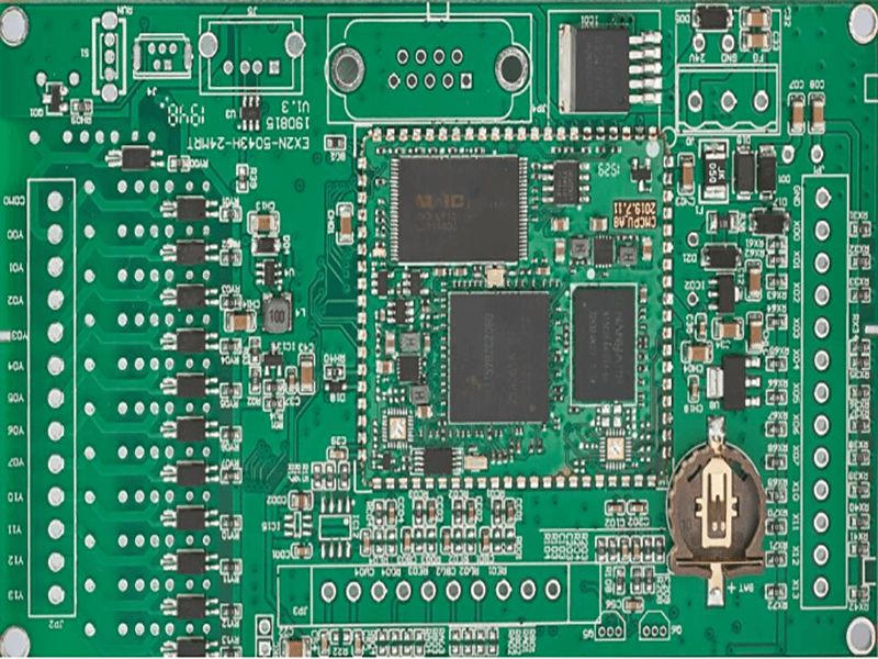
A signal always returns to its source, and at high frequency it returns along the path of least impedance, which is directly beneath the trace. Anything that interrupts that reference, such as a slot, a plane split or a via that changes reference layer, forces the return current to detour and creates a loop that radiates.
Keeping a continuous reference under every controlled impedance line is therefore the most valuable rule in high frequency layout. Where a layer change is unavoidable, a stitching via next to the signal via gives the return current a short path, and the broader principles of suppression are covered in EMI suppression design principles.
Fabrication Challenges
PTFE and similar materials behave differently from epoxy. They are softer, they expand more with temperature, and they are more difficult to drill cleanly, so hole quality and desmear have to be controlled deliberately. Lamination cycles need tighter control of temperature and pressure to avoid resin starvation and thickness variation.
Layer to layer registration matters more than on a digital board, because a lateral shift between a trace and its reference plane changes impedance. Fabricators who build controlled impedance work hold tighter registration and measure the result on coupons, and that capability is a better indicator of suitability than a general capability statement.
Applications and Cost
Radio and microwave links, radar modules, satellite terminals, base station antennas, medical imaging front ends and automotive radar all depend on this class of board. Each of them trades cost against loss, and the acceptable loss figure usually comes from a link budget rather than from the board itself.
Test cost is often underestimated. Verifying a controlled impedance line on every panel needs coupons, and verifying a radio front end needs a measurement setup rather than a continuity check, so the test plan should be agreed early. Cost is driven by the material, the number of layers, the impedance tolerance and the testing. A mixed construction that uses high frequency material only on the signal layers and FR4 elsewhere is a common way to control cost, provided the hybrid stackup is designed so that the two materials do not distort during lamination.
Layer Stackup Choices
The stackup decides how much of the design problem is solved by geometry and how much by material. A two layer board with a grounded coplanar waveguide can work well into the low gigahertz range, but the reference plane is thin and the ground stitching has to be dense. Four layers let the signal sit between two planes, which gives a cleaner return path and better isolation between neighbouring lines.
Above that, the usual pattern alternates signal and plane layers, with the high frequency lines on the outer layers where their impedance can be trimmed by width, and the slower digital buses buried. Symmetry matters as well, because an asymmetric stackup warps during lamination, and a warped panel changes the dielectric thickness across the board and therefore the impedance. The general rules for stackup design are set out in layer stackup from one to eight layers.
FAQ
Can FR4 be used at high frequency? Below about one gigahertz, and where loss is not critical, it can. Above that the drift of its dielectric constant and its higher dissipation factor usually rule it out.
How many layers can a high frequency board have? From a single sided radio board to more than twenty layers in a hybrid construction. The limit is set by the lamination process and by the registration tolerance rather than by the material itself, and a fabricator who can hold registration on a thick hybrid stack is worth more than one who simply stocks the laminate.
What lead time should be expected? Prototypes typically take five to seven working days and volume production two to three weeks, longer where a special material has to be ordered, and the schedule should be agreed before the panel is released because a material substitution made later invalidates the impedance coupon and the test plan that went with it.