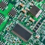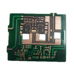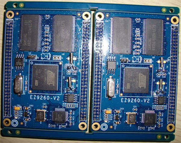
As wireless communication, optical communication, high-speed networking, and advanced electronic systems continue to evolve, PCB technology is facing increasingly demanding electrical and manufacturing requirements. The development of RF front-end modules, high-speed digital circuits, integrated circuits, and microwave systems has significantly increased the need for specialized high-frequency PCB solutions.
Compared with conventional FR-4 circuit boards, high-frequency applications require tighter control of dielectric properties, signal loss, impedance, dimensional stability, and manufacturing accuracy. Material selection must therefore consider not only electrical performance but also processing difficulty, production cost, reliability, and application requirements.
For commercial wireless communication systems, for example, a PCB material may need a stable dielectric constant, low dielectric loss, controlled thickness, and reliable multilayer lamination characteristics. For mobile communication and other compact electronic products, the PCB must also support high integration, fine-pitch interconnects, efficient manufacturing, and long-term reliability.
This article explains the definition of high-frequency PCBs, their applications, commonly used materials, manufacturing processes, and the key challenges involved in high-frequency PCB manufacturing.
What Is a High-Frequency PCB?
A high-frequency PCB is a circuit board designed to transmit or process electrical signals at relatively high frequencies. In general, high-frequency applications begin around several hundred megahertz, while microwave applications commonly operate above 1 GHz. Some advanced systems extend into the millimeter-wave range of tens of gigahertz.
As operating frequency increases, PCB material characteristics become increasingly important. Conventional FR-4 materials may be suitable for many low- and moderate-speed applications, but higher-frequency systems often require specialized high-frequency PCB materials with lower dielectric loss, stable dielectric constant, low moisture absorption, and predictable electrical behavior.
Important material properties include:
- Dielectric constant (Dk)
- Dissipation factor (Df)
- Dielectric thickness
- Copper surface roughness
- Thermal stability
- Dimensional stability
- Moisture resistance
- Mechanical reliability
At high frequencies, even small variations in material properties or transmission-line geometry can affect impedance, insertion loss, phase characteristics, and overall signal integrity.
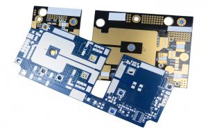
Applications of High-Frequency PCBs
The demand for microwave PCB technology continues to grow as electronic systems become faster, smaller, and more highly integrated.
Common applications include:
- Wireless communication equipment
- RF front-end modules
- Power amplifiers
- Low-noise amplifiers (LNAs)
- Antenna modules
- RF filters
- Couplers and power dividers
- Duplexers
- Automotive radar systems
- Satellite communication equipment
- Aerospace electronics
- High-speed networking equipment
- Industrial RF systems
Automotive radar and advanced wireless communication are particularly important because many of these systems operate at frequencies where PCB transmission-line loss and impedance variations can directly affect system performance.
Classification of High-Frequency PCB Materials
High-frequency PCB materials can be broadly divided according to their resin systems, reinforcement structures, ceramic loading, and electrical characteristics.
Ceramic-Filled Thermoset Materials
Ceramic-filled thermoset laminates combine resin systems with ceramic fillers to provide controlled dielectric properties and low-loss performance.
Representative material families include:
- Rogers 4350B and 4003C
- Arlon 25N and 25FR
- Taconic TLG series
These materials can provide electrical characteristics suitable for many RF and microwave applications while remaining relatively compatible with conventional PCB fabrication methods.
However, their mechanical properties may differ from standard FR-4. Certain ceramic-filled materials can be more brittle, which means drilling, routing, and mechanical processing parameters must be carefully optimized.
Tool wear may also increase during drilling and routing. Therefore, manufacturers should evaluate drill life, feed rate, spindle speed, chip load, and board support conditions before production.
PTFE-Based Materials
PTFE, or polytetrafluoroethylene, is widely used for demanding RF and microwave applications because of its low dielectric loss and stable high-frequency characteristics.
Representative PTFE-based material families include products from manufacturers such as Taconic, Rogers, Arlon, and other specialized laminate suppliers.
PTFE materials are particularly useful when low insertion loss and stable RF performance are critical. However, PTFE-based laminates can be more difficult to process than conventional FR-4 because of their softness, low surface energy, and different mechanical characteristics.
Consequently, PCB processing parameters must be carefully controlled.
PTFE PCB Manufacturing Considerations
Manufacturing a PTFE PCB requires specialized process control from material preparation through final inspection.
1. Material Cutting
During material cutting, protective films should remain in place whenever possible to reduce scratches, dents, and surface contamination.
The cutting process should also minimize mechanical stress because PTFE-based laminates may behave differently from standard rigid PCB materials.
2. Drilling
Drilling is one of the most critical steps in high-frequency PCB manufacturing.
Recommended practices include:
- Use sharp, high-quality drills appropriate for the laminate.
- Optimize spindle speed and feed rate according to hole diameter and material structure.
- Control chip load to prevent excessive heat generation.
- Maintain stable board support during drilling.
- Remove dust and debris from drilled holes.
- Inspect hole walls for resin smearing, tearing, or mechanical damage.
For small holes, drilling parameters must be optimized rather than simply increasing spindle speed. The appropriate combination of spindle speed, feed rate, pecking strategy, and tool life depends on the specific material and hole structure.
Aluminum entry sheets and suitable backing materials may be used to improve drilling stability and protect the PCB surface.
3. Hole-Wall Treatment
PTFE has a relatively low surface energy, making conventional chemical adhesion and metallization more challenging than with standard epoxy-based laminates.
Therefore, specialized surface treatment may be required before electroless copper deposition.
Depending on the material system and manufacturer’s process capability, plasma treatment, sodium-naphthalene activation, or other qualified surface-conditioning methods may be used to improve copper adhesion and hole-wall metallization.
The selected process must be validated for the exact laminate construction rather than applied as a universal recipe.
4. Through-Hole Plating
For PTH structures, reliable copper deposition inside the drilled holes is essential.
After appropriate surface preparation and micro-etching, the PCB proceeds through electroless copper and electrolytic copper plating processes.
Key control factors include:
- Hole-wall cleanliness
- Surface activation
- Electroless copper coverage
- Electrolytic copper thickness
- Current density
- Plating uniformity
- Adhesion between copper and dielectric material
Because PTFE materials present adhesion challenges, insufficient surface activation or inadequate process control can result in poor copper coverage or weak hole-wall adhesion.
Reliable PCB fabrication therefore requires close control of every metallization step.
5. Solder Mask Processing
Solder mask processing for high-frequency boards must balance protection, adhesion, dimensional accuracy, and electrical requirements.
A typical process includes:
- Surface cleaning and preparation
- Solder mask coating
- Pre-baking
- Exposure and development
- Final curing
- Visual and electrical inspection
Mechanical abrasion should be minimized when it could damage the laminate surface or affect the RF structure.
For PTFE-based boards, solder mask adhesion should be verified carefully because the low surface energy of PTFE can make conventional coatings more difficult to bond.
If adhesion defects, blistering, or delamination are detected, the process parameters and surface treatment should be reviewed before mass production.
6. Routing and Mechanical Processing
Mechanical routing, or CNC routing, must be carefully controlled to minimize burrs and surface damage.
When routing PTFE-based materials, the board should be adequately supported and protected. Suitable separator sheets or protective materials may be used to prevent mechanical damage to the copper surface.
After routing, burrs should be removed carefully without scratching the copper or damaging the dielectric material.
Visual inspection should focus on:
- Copper scratches
- Burrs
- Edge damage
- Delamination
- Dimensional accuracy
- Surface contamination
Good routing quality is particularly important for PCB reliability, because mechanical damage can become a source of delamination or conductor failure during subsequent assembly and operation.
High-Frequency PCB Manufacturing Process
The manufacturing flow depends on whether the PTFE material requires non-plated holes or plated through-holes.
NPTH PTFE PCB Process
A typical non-plated-through-hole process may include:
Material cutting → Drilling → Dry-film lamination → Imaging → Etching → Etch inspection → Solder mask → Silkscreen → Surface finish → Routing → Electrical testing → Final inspection → Packaging and shipment
The exact process can vary depending on the layer structure, surface finish, tolerances, and customer requirements.
PTH PTFE PCB Process
A plated-through-hole process may include:
Material cutting → Drilling → Hole-wall treatment → Electroless copper → Electrolytic copper plating → Dry-film imaging → Pattern plating → Etching → Inspection → Solder mask → Silkscreen → Surface finish → Routing → Electrical testing → Final inspection → Packaging and shipment
Additional lamination, via, back-drilling, or multilayer processes may be required for more advanced RF and microwave designs.
Key Challenges in High-Frequency PCB Processing
Compared with conventional PCB production, high-frequency PCB manufacturing presents several important challenges.
1. Copper Plating in Drilled Holes
The inner walls of PTFE-based materials can be difficult to metallize because of their low surface energy and different adhesion characteristics.
Proper hole-wall preparation and activation are therefore essential.
2. Fine-Line Etching and Dimensional Control
High-frequency circuits often require tightly controlled trace width and spacing.
Etching variations can change transmission-line geometry and therefore affect characteristic impedance.
Important control points include:
- Trace width
- Trace spacing
- Copper thickness
- Etching compensation
- Undercut
- Registration accuracy
3. Solder Mask Adhesion
Poor solder mask adhesion can cause blistering, peeling, or contamination during assembly.
This is especially important for PTFE-based materials and mixed-material multilayer boards.
4. Surface Damage
Scratches and dents on RF conductors can affect electrical performance and may create long-term reliability risks.
Manufacturing equipment, work-in-process handling, packaging, and inspection procedures should therefore be controlled carefully.
5. Impedance Control
For RF and microwave circuits, impedance control is one of the most important manufacturing requirements.
Characteristic impedance depends on several factors, including:
- Trace width
- Copper thickness
- Dielectric thickness
- Dielectric constant
- Reference-plane distance
- Trace geometry
- Copper roughness
Therefore, high-frequency PCB materials and manufacturing tolerances must be considered together during PCB design and fabrication.
How to Improve High-Frequency PCB Reliability
Reliable high-frequency boards require cooperation between PCB design engineers and manufacturing engineers.
Key practices include:
- Select materials based on actual operating frequency and loss requirements.
- Define the stack-up before finalizing impedance-controlled traces.
- Maintain consistent dielectric thickness.
- Control copper thickness and surface roughness.
- Optimize drilling parameters for each material.
- Validate PTFE hole-wall treatment before mass production.
- Minimize scratches and mechanical damage.
- Perform electrical testing and dimensional inspection.
- Monitor impedance on controlled-impedance structures.
- Establish material-specific process windows instead of relying on standard FR-4 parameters.
For advanced RF applications, DFM analysis should be performed early so that material selection, trace geometry, drilling, plating, etching, and assembly requirements are considered together.
Kingda’s High-Frequency PCB Manufacturing Support
Kingda focuses on providing PCB manufacturing solutions for demanding electronic applications, including high-frequency and high-speed circuit boards.
For RF and microwave PCB production, manufacturing quality depends on more than material selection. It also requires controlled drilling, reliable copper plating, accurate imaging and etching, stable lamination, solder mask adhesion, impedance control, and comprehensive inspection.
By combining material evaluation with process control and manufacturing verification, Kingda can help customers develop PCB solutions that balance electrical performance, manufacturing feasibility, cost, and long-term reliability.
Conclusion
The selection and manufacturing of a high-frequency PCB require a different approach from conventional PCB production. As operating frequencies increase from wireless communication bands to microwave and millimeter-wave applications, dielectric loss, Dk stability, copper roughness, impedance, dimensional accuracy, and manufacturing tolerances become increasingly important.
PTFE and ceramic-filled materials can provide excellent electrical performance, but they also introduce additional manufacturing challenges, particularly in drilling, hole-wall treatment, copper plating, solder mask adhesion, and mechanical routing.
Successful PCB fabrication therefore requires close coordination between material selection, PCB design, process engineering, and quality control. By optimizing these factors together, manufacturers can produce high-frequency boards with stable electrical performance and improved PCB reliability for next-generation communication, automotive, aerospace, and high-speed electronic systems.