Building a High Quality PCB: Design Priorities
Almost everything that makes a high quality PCB is decided before the board is ordered. The stackup, the copper weight, the surface finish, the tolerances and the test coverage are all choices, and the ones that are made by default are the ones that cost money later. Quality on the board is the result of those decisions being taken deliberately.
The other half is the discipline of checking. A design that satisfies every design rule can still be impossible to assemble, and a board that assembles perfectly can still be untestable. What follows is the order in which the decisions and the checks are usually made.
Design Rules That Match the Supplier
A design rule set is only meaningful if the shop that will build the board can hold it. Minimum trace width, annular ring, solder mask clearance and drill size all have a floor set by the process, and a board that sits below it will either be rejected or built with reduced yield and a hidden reliability cost.
The practical approach is to ask for the supplier’s capability sheet before the layout starts and to enter those numbers into the constraint manager. Routing effort spent on features that will be relaxed later is wasted, and features that the shop cannot hold will come back as a request to change the data.
Material Selection Beyond the Default
The default substrate is a woven glass and epoxy laminate, and it suits most boards. Where the circuit runs fast, sits in a hot environment or has to survive repeated thermal cycles, the dielectric constant, the loss tangent and the glass transition temperature become selection criteria rather than background details.
Material selection also has a cost dimension. A higher performance laminate costs more per panel and often needs a different drilling and lamination recipe, so the decision should be justified by a requirement rather than adopted for safety. The criteria are set out in the discussion of high frequency laminate selection.
Stackup and Copper Balance
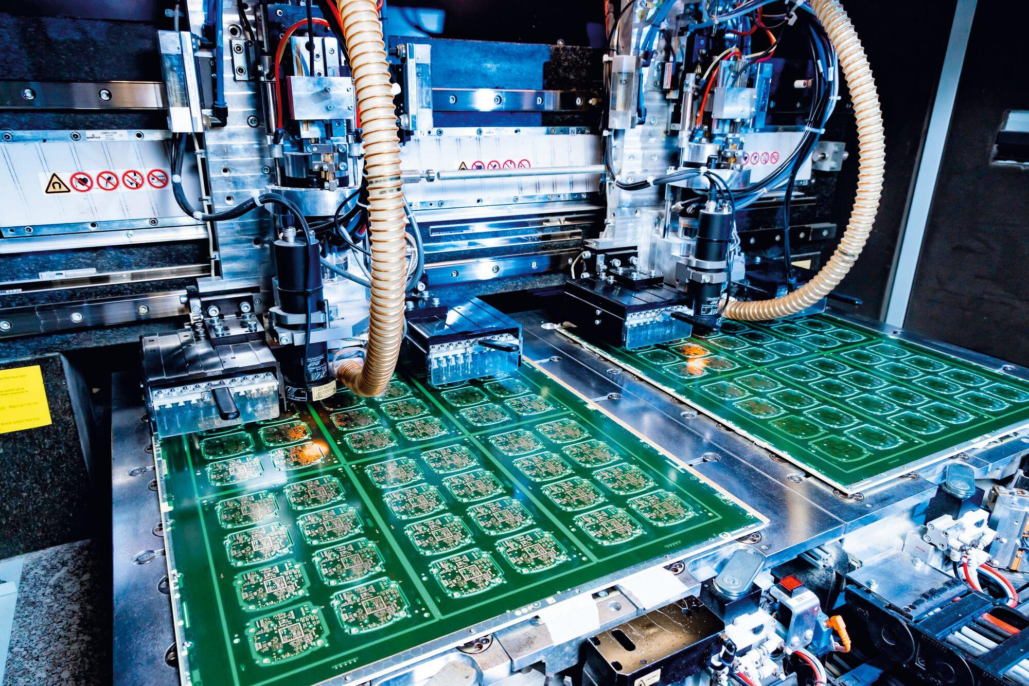
A stackup that is symmetrical in construction and in copper distribution will stay flat through the reflow cycles. A heavy copper plane on one side and a sparse layer on the other builds in a stress that shows up as bow or twist after assembly, and a warped board is difficult to print solder paste onto.
Copper balance is judged per layer as well as between them. Regions of the artwork that are almost empty will etch differently from regions that are dense, which affects the achievable trace width and the impedance of the finished traces. A thieving pattern is the usual way to even out the difference.
Surface Finish and Its Effect on Assembly
The finish protects the copper before assembly and determines how well the solder wets during it. An organic coating is cheap and flat but has a short shelf life and is sensitive to handling. Nickel and gold is durable and flat but adds a step and interacts with some solder alloys. Tin is inexpensive and solderable and has its own ageing behaviour.
For a board with fine pitch features, flatness matters as much as wettability, because the paste deposit depends on the land being level. The finish also determines how the board has to be stored and how long it can wait before assembly, which belongs in the same conversation as the requirements in the component handling plan.
DFM Review Before Release
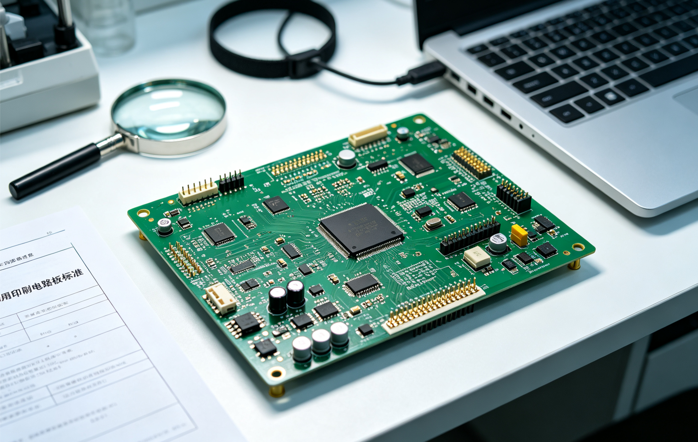
A DFM review is a check of the artwork against the process, and it catches the errors that a design rule check cannot: a pad that is too close to a score line, a solder mask sliver that will lift, a component that shadows its own joint from the convection current in the oven.
The review is worth doing as a conversation rather than as a report. A supplier who understands that a feature is essential and why will often propose a way to build it, while a supplier working from a checklist will simply flag it and stop the order. Both outcomes are better than discovering the problem after the panels are etched.
Test Coverage and Access
Test coverage has to be designed in. In circuit test needs lands of a usable size with a minimum spacing and enough clearance around them for the probe to reach, and those requirements are much easier to satisfy during layout than to add afterwards.
The coverage choice is commercial as well as technical. Testing every unit for every parameter costs money that the product may not need to spend, while testing nothing exposes the customer to escapes. A deliberate mix of a fast structural test on all units and a functional test on a sample is a reasonable compromise for many products.
Documentation That Matches the Board
The documentation is what allows the second build to be identical to the first. A drawing with the stackup and tolerances, an assembly drawing with orientation and polarity, a bill of materials with approved substitutes and a note of any deviation granted during the first build are the components of a complete package.
Deviations are the part most often lost. A stencil adjusted by hand, a part substituted in a shortage, an oven profile tuned for one delivery: each changes the process, and each disappears unless it is written down. The same discipline is described in judging PCB quality.
Panelisation and Breakaway
How the board is arranged on the production panel affects assembly as much as it affects cost. A panel that gives the assembler a rigid edge to clamp, consistent spacing between the boards and enough room for tooling strips will run faster and with fewer placement errors than a panel that packs the boards tightly.
The breakaway method interacts with the layout. V-cut requires a straight line across the panel and leaves a visible edge, while routing with perforated tabs allows curves and mixed shapes but leaves small burrs that have to be planned for. Components near the break line will see the stress of separation, so their placement should account for it.
Assembly Conditions and Rework Access
Assembly conditions are worth reviewing at the layout stage while changes are still free. A tall component placed upwind of a small one in the reflow oven creates a shadow that cools the joints behind it, and a connector placed with its body over the pads of a neighbouring part makes rework of that part almost impossible.
Rework access is easy to overlook and expensive to be without. Leaving a clear path to the pins of a large device, and keeping the thermal mass of the surrounding copper low enough that a repair is feasible, are small concessions that pay off when a unit has to be recovered instead of scrapped once the product is in production and the yield numbers are watched closely.
FAQ
Is a higher performance laminate always better? No. It costs more and often needs process changes. Choose it when the electrical or thermal requirement cannot be met by the standard material.
How much copper imbalance is acceptable? Small differences are normal. A layer that is less than half as dense as the others is a warning sign that should be corrected before the data is released.
When should the DFM review happen? Before the order is placed, and ideally before the layout is frozen, so that the findings can still be incorporated without a re-spin.