High Speed PCB Design: Where Layout Experience Actually Shows
High speed design is not defined by a clock frequency. It is defined by whether the physical path of a signal changes its behaviour, which happens when the rise time is short relative to the length of the interconnect. A slow 100 MHz interface with fast edges can be harder to lay out than a well behaved 1 GHz link, and that is why the discipline is about geometry rather than about labels on a net list.
The practical consequence for a design team is that high speed PCB design work is judged by the questions the engineer asks at the start. Someone who only asks about layer count is preparing to route; someone who asks about references, stackup and return paths is preparing to build something that works.
Reference Plane Continuity Comes First
Every signal returns to its source, and at high frequency the return current follows the path of least impedance, which is usually the plane directly beneath the trace. If that plane is interrupted, the return current has to find another way, and the resulting loop increases inductance, radiates and degrades the waveform.
Reference plane continuity is therefore a placement and stackup problem before it is a routing problem. The sensitive nets should be identified early, the layers they will be routed on should be assigned deliberately, and the places where a plane is split, cut or perforated should be known before the first trace is drawn.
The classic failures are predictable. A connector that forces a split plane across a bus, a power island that interrupts the ground reference under a differential pair, or a via field that perforates the reference beneath a high speed channel. All three are visible on a drawing and painful on a prototype.
Where a reference change is unavoidable, the design should place a stitching capacitor or a controlled transition rather than leaving the return path to chance. That decision is part of the design, not a detail deferred to the manufacturing stage.
Return Path Planning Across the Board
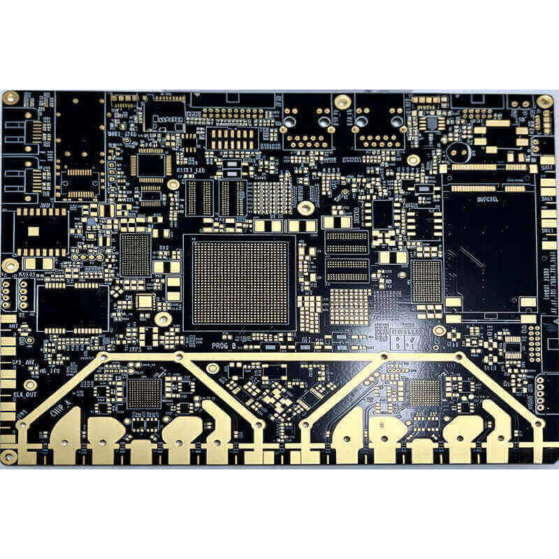
Return path planning extends the same idea to the whole board. Power distribution, analog measurement, switching stages and communication interfaces all have return currents, and the design has to give each of them a path that does not modulate another.
The most common failure in mixed-signal designs is a shared return between a noisy load and a sensitive measurement. A relay coil, a motor driver or a switching regulator sharing copper with a sensor ground produces a measurement that drifts with load, and the fault is often attributed to the sensor or the firmware before the layout is examined.
Planning the return structure before routing means deciding where the ground splits, where the analog and digital regions meet, and how the isolating components are placed so that the return current is guided rather than blocked. Ground splitting without a deliberate plan is usually worse than a single careful plane.
Power integrity belongs to the same conversation. Decoupling placement, plane capacitance and the geometry of the supply path determine whether the voltage at the load stays inside the tolerance the device needs, and the layout of a switching converter is a high speed design problem even when the converter itself is a mature part.
Confirm the Stackup Before Routing
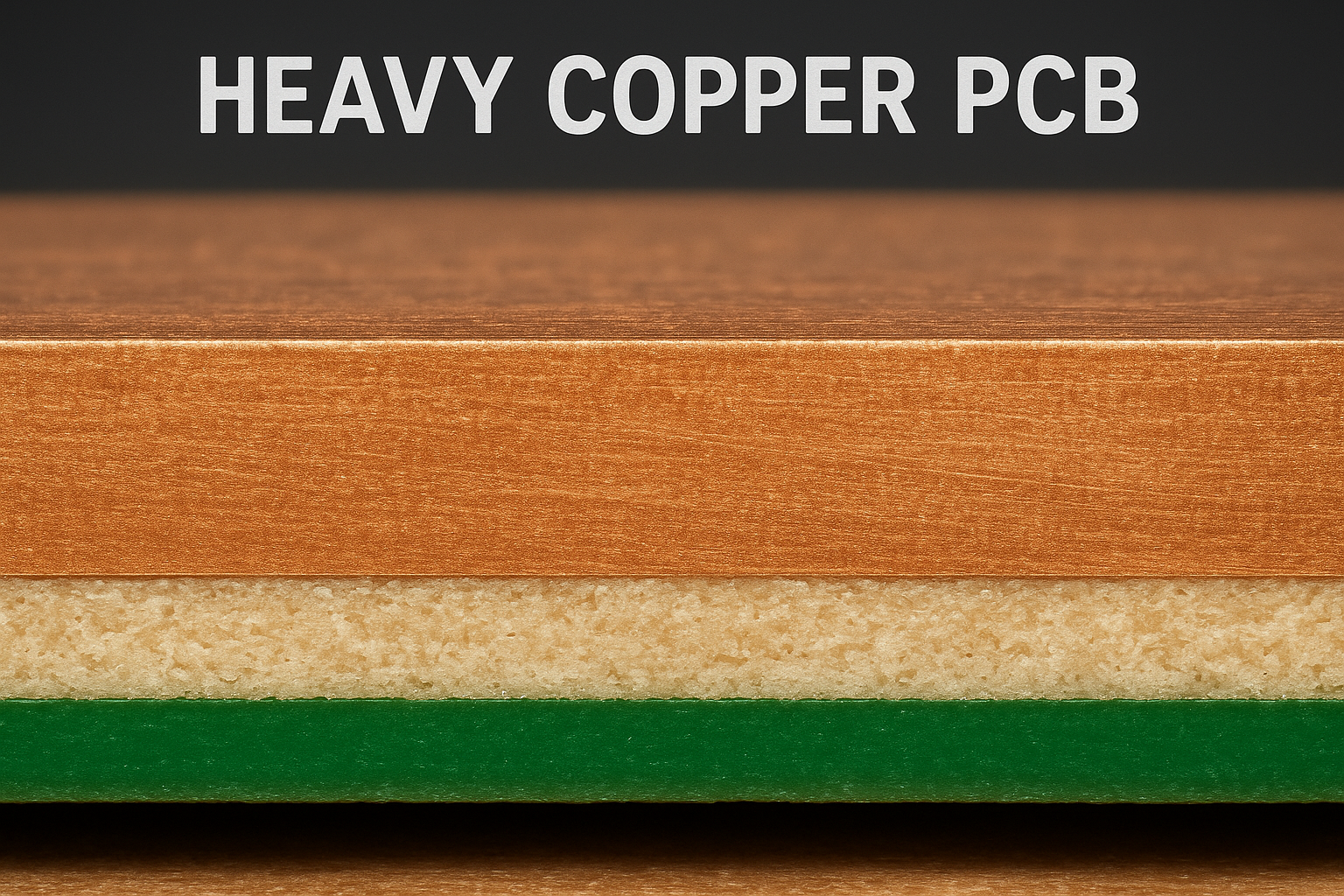
Stackup confirmation is a prerequisite for high speed work rather than a step that follows it. The dielectric thickness between a signal layer and its reference sets the impedance, and the layer order determines which signals can maintain a continuous reference.
There is no universal stackup, and reusing one from another project is a frequent source of problems. The right arrangement depends on the board thickness, the number of layers, the copper weights, the target impedances, the material and the process capability of the factory that will build it.
Where impedance is critical, the fabricator should calculate the trace geometry from the actual material and process rather than accepting a target width from a previous design. The designer then routes to those numbers, which is why bringing the manufacturing partner into the conversation early is a technical advantage and not only a commercial one. A supplier that documents its PCB capabilities as design rules makes that exchange straightforward.
Material choice is part of the same decision. A high frequency laminate behaves differently in the press and during drilling, and a stackup that is correct on paper but awkward to produce will show up as variation between builds rather than as an obvious defect.
Placement Decisions That Decide Signal Behaviour
Placement determines whether the routing can succeed, and in high speed designs it also determines whether the power delivery is realistic.
Devices that communicate with each other should be placed so that the critical channel is short, direct and over continuous reference. Terminations, series resistors and AC coupling capacitors belong close to the source or the receiver according to the topology, not where there happens to be space.
Power components should be placed so that the loop from the input capacitor through the switching device and back is small, because that loop determines both the efficiency and the radiated field. This is one of the few areas where placement matters more than trace width.
Connectors deserve their own review. A connector that forces a long stub, an unavoidable reference change or a crowded escape region will constrain the whole layout, and the decision is often made during the mechanical design rather than during an electrical review.
What the Layout Deliverables Should Contain
The deliverable of a high speed layout is not only a set of Gerber files. The design should be handed over with the stackup and impedance specification, the net class definitions and the rules that were applied, the routing topology chosen for the critical nets and the reason for it, and any simulation or measurement results that support the design.
That package is what allows a later revision to be made without rediscovering the intent, and it is what makes a fabrication or assembly question answerable. Where the same organisation also performs prototype PCB assembly and PCBA testing, the measurement of the prototype completes the record rather than starting a new investigation.
A reviewer should be able to answer three questions from the delivery alone: which nets were critical, what protected them, and how the design was verified.
Reviewing the Design Before Release
- Critical nets identified, with their reference layer named and their continuity checked.
- Plane splits, cut-outs and via fields reviewed against the sensitive routing.
- Return paths for switching currents kept separate from measurement references.
- Decoupling placed against the device pins, with the loop area considered.
- Stackup and impedance confirmed by the fabricator, with a coupon defined.
- Length matching, terminations and via count reviewed for the interfaces that need them.
- Test points placed where a probe can reach them in the assembled product.
FAQ
At what frequency does design become high speed? It is a function of rise time and trace length rather than frequency, which is why fast switching interfaces need attention even at modest clock rates.
Is a ground plane always the answer? A continuous reference is, and a ground plane that is split incorrectly can be worse than a carefully planned structure.
Who should calculate the impedance? The fabricator, from the real material and process. The designer then routes to the resulting geometry.
Can simulation replace measurement? No. Simulation guides the design and measurement confirms it, and the prototype is where the two are compared.
Summary
High speed PCB design is decided by three things: whether every critical signal has a continuous reference, whether the return currents are planned rather than tolerated, and whether the stackup was confirmed before routing began. Get reference plane continuity and return path planning right, keep power integrity in the placement decisions, and treat stackup confirmation as the starting point of the layout instead of the final check.