IC Substrate vs PCB: Structure, Materials and Manufacturing
Two Boards, Two Jobs
An IC substrate and a printed circuit board look similar from a distance: both are laminates with copper layers, vias and solder resist. In practice they operate at completely different scales. A PCB carries components between one another across centimetres; an IC substrate carries the connections between a semiconductor die and the package pins across millimetres, with a density that a conventional PCB process cannot reach. The distinction matters because the design rules, the materials and the manufacturing methods are fundamentally different, even though the underlying idea is the same.
What an IC Substrate Is
An IC substrate, also called a package substrate, sits inside the chip package. The die is mounted on its top surface, wire bonded or flip chip attached, and the substrate fans the die’s connections out to the ball grid array on its underside, which then solders to the PCB. It also provides mechanical support, distributes power to the die and, in advanced packages, may integrate multiple dies or a passive interposer. Because the die’s pads are extremely fine, the substrate has to hold line widths and spaces far below what a PCB can manage, and it has to match the thermal expansion of silicon closely enough to survive thousands of temperature cycles.
What a PCB Is
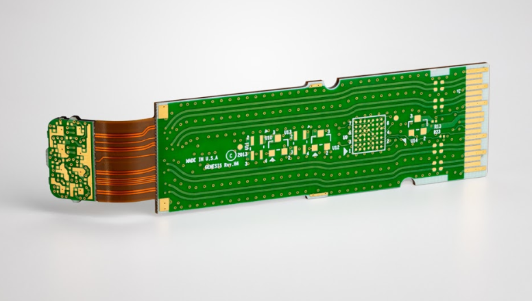
A conventional PCB is the board that carries the finished packages, connectors, passives and power components. It is fabricated from glass reinforced laminate, drilled with mechanical or laser holes, plated and patterned with lines and spaces that typically range from 100 microns down to about 40 microns in fine line work. It is designed to be robust, repairable and relatively inexpensive, and it operates at a scale where 0.1 mm is a small feature rather than a large one.
The Key Differences
Line width and spacing. A PCB holds 40 to 100 micron lines in production; an IC substrate works at 2 to 10 microns, and advanced packages go below that. Via size. PCB vias are measured in tenths of a millimetre; substrate microvias are 30 to 50 microns, made by laser. Layer count. Most PCBs use two to eight layers, while a package substrate for a large processor can use ten to twenty layers built up in repeated cycles. Size. A substrate is often only a few centimetres on a side, sized to the package. Dielectric material. PCBs use woven glass reinforced epoxy; substrates use glass free resin systems such as BT resin or build-up films, because glass weave would disturb the fine geometry and the electrical properties. CTE. The substrate must be engineered to match silicon, whereas a PCB is designed to match the components and connectors mounted on it. Volume. PCBs are made in panels containing many boards; substrates are made in panels containing many packages, and are handled in a class of cleanliness closer to semiconductor processing.
Materials
Substrate materials fall into a few families. BT resin is a common choice for wire bonded and moderate density packages because it is rigid, has a controlled CTE and holds fine lines well. Build-up films based on epoxy or polyimide are laminated over a core to form the fine pitch layers on top of a coarser core, which is what makes the layer count possible. Coreless substrates remove the central core entirely for the thinnest packages, using the build-up layers alone for support. Advanced packages may use molded or fan-out structures where the die is embedded in a reconstituted wafer. The common thread is that all these materials are chosen for dimensional stability, low warpage and dielectric properties at high frequency, not for cost.
Manufacturing Differences
Both start from panels and build layers, but the process windows diverge. Substrate fabrication uses semi-additive or modified semi-additive processing to achieve fine lines, laser drilled microvias with small capture pads, and build-up dielectric films applied by lamination rather than glass fabric impregnated with resin. Warpage control becomes a first order problem, because a thin substrate with many build-up layers will bow if the copper balance and the cure profile are not matched. Inspection also differs: the features are small enough that optical inspection and electrical test must be adapted from the PCB world, and yields are measured on features that a PCB shop would not even attempt.
Cost and Where the Boundary Sits
An IC substrate costs many times more per unit area than a PCB, and its cost scales with layer count, line width and panel yield. That is why the boundary between the two is a matter of economics as much as technology: work is pushed down to the PCB when the density allows, and up to the substrate only when the die requires it. The practical consequence for a product designer is that the PCB and the package are designed together, since the escape routing on the substrate and the fan-out on the board have to meet at a ball pitch that both can handle.
The two technologies meet at the package boundary, so they should be planned together. Review how PCB manufacturing handles the fine line and via rules on the board side, apply realistic escape routing in your PCB design and layout, and check the design and manufacturing considerations before release. A prototype PCB assembly run with the real package confirms that the fan-out and the BGA footprint agree.
FAQ
Is an IC substrate just a high density PCB? No. It uses different materials, glass free dielectrics, laser microvias and build-up processes, and it must match the thermal expansion of silicon.
Why do substrates avoid glass weave? Because the weave creates local variation in dielectric constant and mechanical properties that disturb micron scale features.
Why is CTE matching so important for a substrate? Because the die is rigid and brittle, and thousands of temperature cycles will crack the joints if the substrate expands differently.
Can a normal PCB shop make an IC substrate? Generally no. Substrate fabrication needs laser via capability, build-up lamination and fine line processing beyond standard PCB equipment.
Conclusion
An IC substrate and a PCB share a laminate construction but operate at different scales and for different purposes. The substrate connects a die to the package with micron features and must match silicon; the PCB connects the packages with features measured in tens of microns and must be robust and economical. Design them together at the package boundary, keep the board side inside the achievable fine line rules, and the interface between the two will work in 2026.