IGBT Control Board Design for Induction Heating
An induction heating power supply is a switching converter that happens to drive a coil instead of a transformer, and the board that generates the switching pattern is the heart of it. An IGBT control board has to produce two complementary pulse trains at a frequency that tracks a resonant tank, keep the two halves of the bridge from conducting at the same time, and shut the converter down cleanly the moment current or voltage leaves its safe range. Units in this class cover roughly 10 to 120 kilowatts, and at those power levels a control mistake destroys hardware rather than producing a warning.
What the System Looks Like
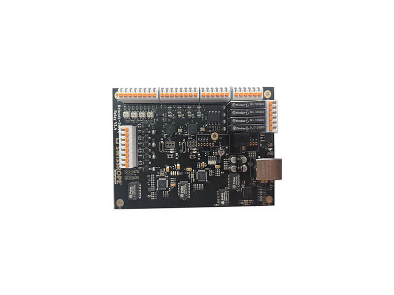
A typical induction heating unit is built from three boards rather than one. A front panel handles operator interface and indication. A main control board generates the switching signals, manages protection, and interfaces to the sensors. Two driver boards sit close to the power stage and translate the low-level logic signals into isolated gate pulses for the IGBT modules.
Separating the control board from the driver boards is not an aesthetic decision. The power stage switches hundreds of amperes in tens of nanoseconds, and the resulting dV/dt couples into anything sharing a ground with it. Keeping the logic at arm length, with an isolation barrier between the two domains, is what makes the control board reliable in the first place.
How Induction Heating Loads the Bridge
The work coil and a capacitor network form a resonant tank driven by a bridge of IGBTs. In a series-resonant arrangement the current is sinusoidal and the bridge switches near the zero crossings, which keeps switching loss low. In a parallel-resonant arrangement the tank presents a different impedance, and the bridge sees a current waveform that is closer to square. Either way the tank impedance is a strong function of frequency, and the converter has to operate near resonance to deliver power efficiently.
That gives the control board its first real job: it must run at a frequency that keeps the tank in the right region even as the workpiece heats, changes permeability, and shifts the resonant point. Fixed-frequency operation is only acceptable where the load is repeatable and the tank is designed with enough margin.
Pulse Generation
The bridge needs two gate signals that are almost, but not exactly, complementary. Pulse generation is usually built around a dedicated PWM controller or a timer in a microcontroller, configured to produce a defined frequency range with the two outputs separated by 180 degrees. The output frequency band for this class of equipment is typically 20 to 60 kilohertz, set by the tank and by the switching capability of the devices.
The critical parameter is dead time. Both devices in a bridge leg must be off for a short interval while the other turns on, otherwise the DC link is shorted through the leg and the resulting current spike destroys both devices. Dead time has to be long enough to cover the turn-off time of the slowest device and the propagation delay spread of the gate drive circuit, and short enough not to distort the output waveform. It is usually fixed in hardware rather than left to software, because software cannot guarantee it under every condition.
Gate Drive
The gate drive chain is where most design effort goes. Each high-side device needs an isolated supply, because its emitter sits on a node that swings between the DC link rails. The isolation barrier carries not just power but also the fast switching transients of the power stage, so the barrier’s common-mode transient immunity is a specification that matters as much as its voltage rating.
Gate resistors are chosen as a compromise. A small turn-on resistor speeds up switching and reduces loss, but raises dV/dt and the resulting electromagnetic emissions; a larger turn-off resistor slows the current fall and reduces voltage overshoot across the device. Many designs use separate resistors for turn-on and turn-off, plus a diode path, so that the two edges can be tuned independently. A negative bias during the off state is common on larger modules, because it increases margin against spurious turn-on when the opposite device switches and injects current through the Miller capacitance.
Physically, the gate loop must be small. The gate drive return should run alongside the gate trace and, where the device is a module, an auxiliary emitter terminal should be used as the return reference so that the voltage drop in the main emitter path does not subtract from the applied gate voltage.
Protection Functions
Protection is not an add-on in this application; it defines whether the equipment survives a fault. The first layer is overcurrent protection, with a threshold that the operator can adjust, because the acceptable current depends on the workpiece and the coil. Detection is usually by current transformer or a shunt in the DC link, with a comparator that trips the drive within microseconds.
Desaturation detection is the second layer and it protects the device rather than the load. When an IGBT is on and its collector-emitter voltage stays high, the device is carrying more current than it can sustain, and the only safe response is to turn it off slowly and latch the fault. This is a per-pulse function, which is why it belongs in the gate drive rather than in the controller.
Overvoltage protection covers the DC link and the output, and it matters most when the load is removed or the tank becomes mismatched, because the resonant voltage can rise well above the supply. Phase loss, undervoltage, and cooling faults are the remaining inputs: a water-cooled coil that loses flow will overheat within seconds, so a flow switch and a temperature sensor are both wired into the trip chain. Each fault should latch rather than auto-reset, so the operator sees the cause rather than a machine that restarts into a fault repeatedly.
Layout Practice
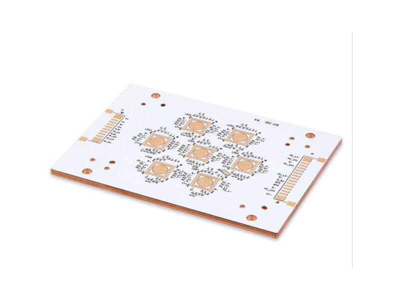
The control board layout is dominated by keeping the noisy and the sensitive apart. The gate drive loops live on the driver boards next to the devices. On the control board, the analogue measurement section, the logic, and the interface to the driver boards should each have their own reference area, joined at a single point rather than poured together, which follows the same ground and power trace planning principle used on mixed-signal boards. Current sense signals should be routed as pairs and kept away from the gate signal runs.
The DC link is the other layout priority, and the same loop-area discipline that governs a dc-dc converter layout applies here at far higher current. The loop formed by the link capacitors and the bridge devices carries the full switched current, and its area determines the voltage overshoot the devices see. Film capacitors placed directly across the bridge terminals, with short wide connections, are the standard answer, and a snubber across each device adds margin where the layout cannot be made tight. Track widths on the power path should be sized from the RMS current with a temperature-rise allowance rather than from habit, since a conductor carrying tens of amperes with a poor thermal path will run hot even if its nominal current rating looks adequate, which is why trace width and current capacity should be calculated from the RMS value plus a temperature-rise allowance.
Thermal Design
Power modules in this class are mounted on a water-cooled heatsink, and the thermal path is part of the electrical design rather than a mechanical detail. Thermal interface material thickness and flatness matter, as does the location of the temperature sensor, which should sit where it sees the baseplate rather than the air. Water-cooled systems usually monitor flow or pressure as well as temperature, because a blocked channel produces a local hot spot that a baseplate sensor will not see quickly enough.
Commissioning
Bring-up follows a fixed sequence. Verify the drive waveforms into a dummy load first, checking frequency, dead time, and the shape of the gate voltage, then confirm that protection trips on a simulated fault. Power up at reduced DC link voltage with a low-power workpiece before running at rating. Check the tank current waveform for the expected shape and measure device case temperature at steady state rather than after a few seconds. Only then run at full power, logging current and temperature throughout, because the failure mode that damages hardware appears as a slow temperature rise rather than as an immediate event.
FAQ
Why is dead time fixed in hardware? Because it has to be guaranteed under every operating condition, including faults and interrupts. Software can introduce jitter and, in a failure, can stop updating entirely, which is exactly when a shoot-through is most likely.
What power range does this class of control board cover? Roughly 10 to 120 kilowatts, with output frequencies of about 20 to 60 kilohertz depending on the tank and the devices.
Is a separate driver board necessary? It is the practical arrangement above a few kilowatts. Isolation and short gate loops are easier to achieve when the drive circuit sits next to the power devices instead of several centimetres away.
What is the most common cause of failure during development? Insufficient dead time and an oversized DC link loop. The first destroys both devices in a leg, the second destroys them through voltage overshoot at turn-off.