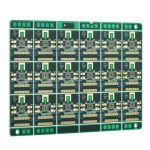
Impedance Mismatch In High Speed Routing: What Causes It
A high speed link is designed as a transmission line, and a transmission line only behaves as designed when its impedance is the same from end to end. Every place where that uniformity breaks becomes a source of signal reflection, and the reflected energy returns to the driver, interferes with what follows, and shows up as overshoot, ringing or a closed eye. The causes are usually small features that were not considered part of the signal path.
This article describes the most common sources of impedance mismatch in high speed routing, why each one matters, and how to deal with it during layout.
Most of these features have to exist in some form. A component has to be soldered to a pad, a signal has to change layers, and a bus has to be routed on the board that exists. The design question is which form creates the least disturbance.
What A Mismatch Does To The Waveform
When a wave travelling along a line meets a change in impedance, part of its energy continues and part is reflected back toward the source. The proportion depends on the size of the change: a small discontinuity returns a small reflection that may still leave enough margin, while a large one can dominate the eye diagram. Repeated discontinuities compound the problem, because each one adds another reflection with its own delay.
The visible symptoms are overshoot at the receiver, ringing that takes time to settle, and a reduction in the amplitude available at the sampling instant. In a differential link the same mechanism can also convert part of the differential signal into a common mode component, which radiates and which the receiver rejects.
<img src="https://www.gopcba.com/wp-content/uploads/2026/01/Макро-изображения-поверхности-PCB-с-покрытием-ENIG.jpg" alt="High speed differential pair routed across a multilayer board” />
Pads, Narrow Traces And Interface Connectors
The impedance of a trace depends on its width and on its distance to the reference plane, and the same relationship applies to the pad it connects to. A large pad presents a low impedance, while the narrow trace that feeds it presents a higher one, so the junction between them is a step. The larger the pad relative to the line, the bigger the step.
The usual remedy is to control the environment under the pad. Placing a keep out of copper on the layers beneath the pad, with a reference plane on a layer further down, raises the local impedance and brings it closer to the value of the line. The same treatment is used at interface connectors, where the pad is large for mechanical reasons and cannot simply be reduced. Reviewing these transitions during the artwork check catches the ones that were missed.
Vias And Layer Transitions
A via is a vertical section of the signal path, and it is almost never the same impedance as the horizontal line it joins. It also carries a length of unused barrel, known as a via stub, below the layer where the signal leaves it. That stub behaves as a short open circuited line, and at frequencies where its length approaches a quarter wavelength it turns into a strong notch in the response.
Removing the stub, or keeping it short enough that its resonance is far above the band of interest, is the first fix. The second is to give the transition somewhere to return its current by placing ground vias close to the signal via, and to avoid long stretches where the reference plane changes. In dense boards, the design rules for vias are usually written around exactly these two concerns.

Corners, Stubs And Branches
A right angle corner in a wide trace is a small impedance discontinuity, because the copper available at the corner is greater than along the straight sections. The effect is modest but real on wide traces and at high frequency, and the conventional answer is to use two forty five degree bends instead of one ninety degree bend, or a curved bend where the layout allows.
Branches are a larger concern. A trace that splits to reach two loads presents a stub to whichever load is further away, and a resistive pull up placed a long distance from the line it serves creates the same problem. Where a stub is unavoidable, keeping its electrical length short relative to the rise time of the signal limits the harm. A routing decision that looks harmless on a schematic can therefore matter a great deal at speed.
Differential Pairs And Reference Planes
A differential pair has to be routed with the width and spacing that produce the intended differential impedance, and any deviation along the run changes it. The pair should be kept symmetric, and the two traces should see the same environment, because asymmetry is what converts differential energy into common mode energy.
The reference plane matters as much as the traces. A continuous plane under the pair gives the return current a defined path that follows the trace. A slot, a plane split or a group of dense via antipads in that plane forces the return current to detour, which changes the impedance of the line above it and creates radiation at the same time. Where a split cannot be avoided, the crossing should be bridged with stitching capacitors or redesigned.
Rules That Depend On The Interface
Different interfaces carry different requirements, and the layout rules follow from them. A universal serial bus pair is usually routed as a differential pair with a defined width and spacing, and the spacing between separate pairs is kept larger than the spacing within a pair. Video links impose a similar structure with a larger gap between pairs, and low voltage differential signalling defines its own differential impedance with a tolerance.
Memory interfaces add a different class of requirement, because the data lines have to be matched in length as well as impedance. The general principle is the same in every case: decide the target impedance for the interface, keep it constant along the path, and treat every feature that interrupts it as something to be justified rather than accepted. gopcb builds controlled impedance boards with documented stackups so that the value the simulation used is the value the board presents.
When a link fails its eye mask on the bench, the useful approach is to work from the largest discontinuity to the smallest. The largest is usually the connector or the package launch, where the geometry is fixed by a standard; next come the layer transitions, where the number of vias can be reduced or the stub shortened; the smallest are the corners and the short branches. Attacking them in that order means each change can be measured before the next is attempted, instead of changing several things at once and learning nothing.
FAQ
Does a short via really matter? It can. A stub is a resonant structure, and its effect grows quickly as the frequency rises. Shortening it is one of the cheapest improvements available.
How large a discontinuity is acceptable? There is no single number. The answer depends on the rise time of the signal and on the margin the interface provides, which is why the same feature can be harmless in one design and fatal in another.
Can the reference plane be split without a penalty? Not for a high speed trace. The return current has to follow the trace, and a split forces it to detour, which changes the impedance and radiates.