Laser Processing in PCB Manufacturing: Cutting, Drilling, Depaneling
Laser processing entered PCB manufacturing as a way to solve problems that mechanical tools handle poorly: very small holes, shapes that a router cannot follow, and panels that cannot tolerate mechanical stress. It is now used across drilling, cutting, depaneling and direct imaging, and the choice of laser wavelength is what determines whether a given material can be processed cleanly.
Where Lasers Are Used
The main applications are microvia drilling, profile cutting and depaneling, and direct imaging of the resist. In each case the laser replaces a mechanical process that is either too coarse, too slow, or applies force to the board. Because the process is non-contact, it produces no mechanical stress and no tool wear, and it can follow any contour that the program defines.
The advantages are consistent across those applications. Cutting is not limited to straight lines, tooling does not wear out, and a new shape is a program change rather than a new die. That last point changes the economics of small batches: where a mechanical process needs a die that must be amortised over thousands of boards, a laser needs only a file. Setup time falls accordingly, which matters most for prototypes and small batches where tooling cost dominates.
Speed is the other practical difference. Because the beam is positioned by a scanner rather than by a moving table, the cut can follow a complex contour without the acceleration limits that constrain a router. The same scanner allows a small feature to be produced inside a large panel without repositioning the work, which keeps the panel handling to a minimum.
Wavelength and Material Interaction
Carbon dioxide lasers operate in the infrared and are effective on organic materials such as FR-4, where the energy is absorbed by the resin. Their limitation is the heat they deposit: the material is removed by thermal means, which can char the edge and create a heat-affected zone. That is acceptable for some profiling work and unacceptable where a clean edge or a fine feature is required.
Ultraviolet and green lasers work by a different mechanism. Their shorter wavelength and shorter pulse width break the material bonds directly rather than heating it, so the heat-affected zone is very small and charring is largely absent. They also couple into a wider range of materials, including glass fibre, copper foil and most laminate types, which makes them the practical choice for fine work.
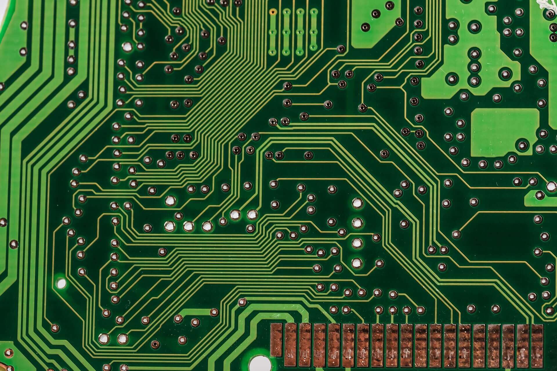
The result of that difference is visible in the quality of the cut and in what the process can produce.
Cutting and Depaneling
Laser cutting produces an edge that is smooth and free of burrs, with no dust and no mechanical stress on the panel. Because the beam can follow any contour, curved outlines, internal cut-outs and slots that would be difficult to rout are straightforward. Cutting with camera-based positioning holds the kerf below about 50 micrometres and places the cut accurately relative to the circuit pattern, which matters when the cut runs close to copper.
Depaneling is a natural application. The alternative methods, V-score and routed tabs, apply mechanical force, and that force is what damages brittle components near the separation line. Laser separation avoids the force entirely, which is valuable on boards carrying ceramic capacitors, crystals or thin packages close to the edge. The design consequence is that the breakaway geometry can be simplified, as long as the panel still supports the board through the line and the slot and edge routing rules are respected.
Laser Drilling of Microvias
Microvia formation relies on the same mechanism. A CO2 laser can drill through the resin of a thin dielectric but stops at the copper below, because the copper reflects the infrared beam. That self-limiting behaviour is useful for blind vias, where the depth is defined by the copper layer beneath the dielectric rather than by a depth setting on the tool.
UV lasers are used where the dielectric is thin and the via must be small, and where a copper surface has to be opened before the dielectric is removed. The combination of the two processes is common in HDI board fabrication, and the drill program has to account for the different behaviour and the different achievable diameters of each.
Advantages Over Mechanical Processing
The practical advantages are worth listing because they explain where the process earns its cost. Because processing is non-contact, the board is not deformed and no stress is introduced. Because there is no tool, there is no tool wear, no breakage and no re-sharpening, and the machine can process hard and soft materials with the same program. Because the shape comes from software, any contour can be produced without a die, which removes the tooling investment and shortens the time from drawing to part.
Material utilisation improves as well, because parts can be nested by program rather than by a fixed die layout. Waste is reduced, and the machine footprint and noise level are lower than those of mechanical alternatives.
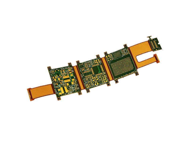
The limitations are just as real, and they decide when a laser is not the right tool.
Limitations and Process Control
Heat management is the main constraint for infrared processing. Even with a short pulse, some energy is absorbed as heat, and the surrounding material can be affected if the parameters are wrong. Pulse energy, repetition rate, focus position and the number of passes all interact, and the process window is narrower than it first appears. For a material with a low decomposition temperature, or for a board with a solder mask that discolours easily, the margin is smaller still.
Copper thickness is the other limit. A thin copper foil can be cut, but a heavy copper layer requires much more energy, and the edge quality falls. Where a design combines a thick copper plane with a laser-processed outline, the process has to be validated on a sample rather than assumed from the general capability.
What Designers Should Provide
Laser processing still needs a defined outline and a defined panel. The mechanical drawing should state the outline, the slots, the cut-outs and the tolerances, and the panel should carry the fiducials needed for camera positioning. The board outline and mounting features define what the laser will follow, and the separation method should be agreed with the fabricator rather than left to the shop floor.
A brief note in the fabrication drawing stating which features are laser processed, and to what tolerance, prevents the shop from applying a general default. As with any special process, the requirement should be measurable, and the first article should be inspected against it.
Cost should be assessed over the whole programme rather than per board. A laser process may carry a higher hourly rate than a router, but it removes tooling, reduces handling, improves material utilisation and shortens the time to a first article. On prototypes and small production runs those savings usually dominate, and on large runs the comparison depends on the feature size the design actually requires.
FAQ
Is laser cutting suitable for all PCB materials? Most laminates can be processed, but the parameters differ. Materials with low decomposition temperatures and heavy copper layers need validation on a sample before the process is committed to production.
Why is UV preferred for fine features? The shorter wavelength removes material by bond breaking rather than by heating, so the heat-affected zone and the risk of charring are much smaller, and the achievable feature size is finer.
Does laser depaneling remove the need for breakaway tabs? It removes the need for a mechanical separation step, but the panel still has to support the board through assembly. The tab or slot design has to satisfy both requirements.