Machine Vision PCB: Sensor Interface and Power Noise
A machine vision board exists to move image data from a sensor to a processor without corrupting it. That sounds simple, and it becomes difficult because the data rate is high, the sensor is sensitive to its supply and its clock, and the processor that consumes the data is a source of noise that can degrade the very signal it is trying to read.
This article covers the blocks on a machine vision PCB, the interface requirements that dominate the layout, and the measures that keep image quality predictable.
What Is on a Vision Board
The sensor is the centre of the design, whether it is a small area sensor on a fixed camera or a large line-scan device on an inspection system. Around it sit the interface logic, the processor or the FPGA, the memory that buffers the frames, the power architecture and the interfaces to the host and to the lighting.
Many designs also include a trigger input and a strobe output, because the exposure has to be synchronised with the movement of the object being inspected. Those signals are slow but their timing is critical, and they have to be routed so that their delay is predictable relative to the sensor timing.
The Sensor Interface
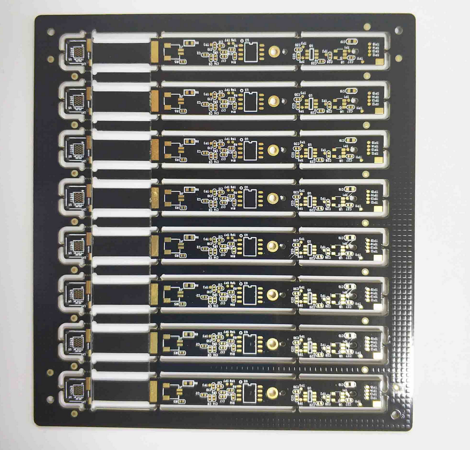
An image sensor interface presents its data on a wide parallel bus, on a set of high-speed serial lanes, or on both. The serial interface is the more demanding, because each lane carries data at a rate where the interconnect behaves as a transmission line and the timing budget is measured in picoseconds.
The sensor manufacturer normally specifies the trace geometry, the length matching and the reference plane requirements, and those specifications should be followed exactly rather than adapted. The supply and the clock for the sensor are equally critical: a noisy supply appears as noise in the image, and a jittery clock appears as a variation in the sampling instant. The high-speed interface layout rules describe how the lanes and the clock should be arranged.
Bandwidth and Stack-Up
Image data rates exceed the capacity of a modest stack, so the layer count is usually set by the sensor interface rather than by the processor. A board carrying several serial lanes plus the memory interface typically needs eight or more layers, with the high-speed lanes on layers adjacent to a solid ground plane.
The differential pairs that make up the serial lanes have to be routed with a constant spacing and a matched length, because any skew between the two conductors converts part of the signal into a common-mode component that radiates and reduces the eye opening. The stack also has to provide a quiet reference for the analogue section of the sensor and a low-impedance path for the digital return currents. Those two requirements are not always compatible on a small board, and the layout usually separates them by area rather than by layer. The mixed-signal layout rules describe how the analogue and digital returns should be arranged when they share a board.
Power Noise and Image Quality
The sensor’s analogue supply sets the noise floor of the image. Any ripple on that rail appears as a pattern in the output, and because the ripple is correlated with the digital activity, the pattern moves with the scene rather than staying fixed. That makes it far more damaging than random noise in a measurement application.
The remedy is a dedicated, heavily filtered supply for the sensor, derived from a linear regulator rather than from a switching one where the current allows. Where a switching regulator is necessary, its output should be filtered and its switching frequency chosen to avoid the sensor’s sensitive bands. The trace width and current calculation gives the geometry for the supply paths, and the supply to the sensor should be laid out as a short, wide path with local decoupling at the sensor pins.
Clocking and Timing
Clock distribution is where many vision designs fail. The sensor clock, the interface clock and the processor clock have different requirements, and each has a jitter budget that the layout can consume if the trace is routed carelessly. A clock that passes near a switching supply or that shares a return path with fast data will pick up jitter that no amount of software filtering can recover.
Clock traces should be routed as controlled-impedance lines with a continuous reference plane, kept away from the power section, and terminated where the topology requires it. Where a clock has to fan out to several devices, the skew between the branches has to be controlled, because skew between the clock and the data directly reduces the timing margin.
Thermal Design
The processor and the sensor both dissipate power, and both have parameters that drift with temperature. In a vision system the two effects combine: a warm sensor has a higher dark current, and a warm processor has a lower timing margin.
The thermal path should carry heat away from the sensor rather than through it. Placing the processor on the opposite side of the board, or at least away from the sensor, keeps the sensor at a more uniform temperature, which matters for a measurement system where the image is compared against a reference. Consistent temperature also makes the calibration more stable, because the sensor’s response changes with temperature even when the illumination is constant.
Mechanical Alignment
The sensor has to be positioned relative to the optical axis to a tolerance far tighter than the board outline tolerance. That is normally achieved with a mechanical feature rather than by the board itself, since the sensor mounting holes and the board outline cannot both hold the required accuracy.
The board’s job is to allow that alignment to happen. The layout should provide for the sensor mounting features, allow for the adjustment range, and keep copper and components clear of the optical path. Where a lens holder is mounted on the board, the copper balance around it matters because an unbalanced stack can bow and tilt the assembly.
FAQ
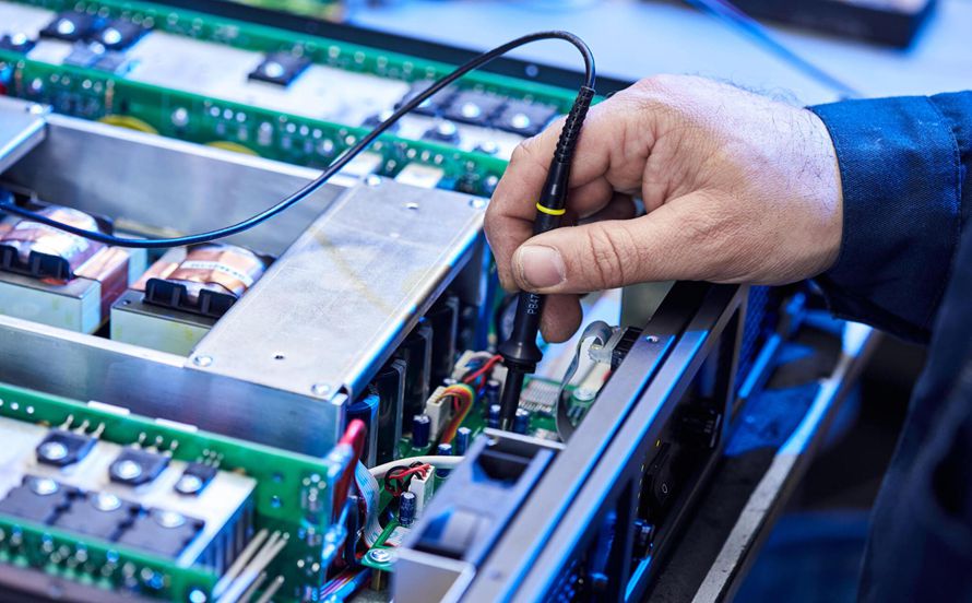
Why does my image show a moving pattern? A pattern that moves with the scene is usually coupled noise rather than a sensor defect. The most common sources are the sensor supply and the clock, and the layout around the sensor should be examined first. Measuring the supply ripple at the sensor pins with a wideband probe, while the processor is running a worst-case workload, usually identifies the coupling path within a few minutes.
How many layers does a vision board need? Enough to route the sensor interface with a continuous reference plane and to separate the analogue and digital sections. That is usually eight layers for a board with serial lanes, and more where a large memory interface is also present. The layer count is driven by the escape from the sensor and the processor packages, not by the number of nets, so the useful exercise is to plan the fanout before choosing the stack.
Can the processor share the board with the sensor? It usually does, and the layout has to separate them. The processor belongs on the side away from the sensor, with the ground plane continuous between them and the switching supplies placed as far from the sensor supply as the board allows.