Medical PCB Manufacturing Diagnostic Equipment Precision & Reliability
Medical diagnostic equipment—including CT scanners, MRI systems, ultrasound equipment, biochemical analyzers, patient monitoring systems, and laboratory instruments—depends on highly reliable electronic systems to deliver consistent performance.
At the center of these systems is the Medical PCB, which provides the electrical interconnection between sensors, processors, power circuits, communication interfaces, imaging modules, and other critical electronic components.
Compared with PCBs used in general consumer electronics, medical diagnostic equipment PCBs often require tighter control of electrical performance, dimensional stability, signal integrity, reliability, cleanliness, and manufacturing consistency.
For this reason, Medical PCB Manufacturing is not simply a matter of producing circuit boards according to Gerber files. Material selection, circuit fabrication, drilling, lamination, surface finishing, inspection, and assembly must work together as a controlled manufacturing process.
GOPCBA provides PCB fabrication and assembly solutions for medical electronics, supporting multilayer, HDI, flexible, rigid-flex, high-TG, high-frequency, controlled-impedance, and other advanced PCB technologies.
Material Selection for Medical Diagnostic PCBs
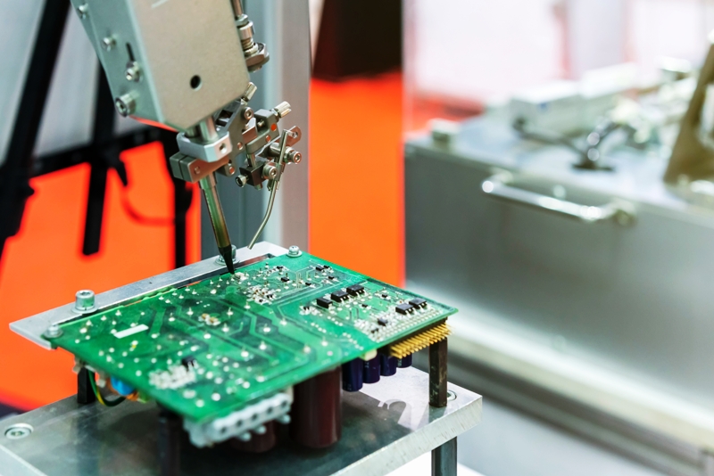
Material selection is one of the first and most important stages of Medical PCB Manufacturing.
Medical diagnostic equipment can operate continuously for extended periods and may process sensitive analog, digital, RF, or high-speed signals. The PCB material therefore needs to provide stable electrical and mechanical characteristics under the intended operating conditions.
Depending on the application, engineers may evaluate:
- FR-4 and high-TG laminates
- Low-loss high-frequency materials
- Polyimide materials
- Flexible PCB materials
- High-reliability multilayer laminates
- Controlled-impedance materials
- Specialized dielectric materials
Electrical Performance and Signal Integrity
Diagnostic equipment can contain sensitive signal acquisition circuits where electrical noise and signal loss can affect system performance.
For high-speed or high-frequency circuits, dielectric constant, dissipation factor, copper roughness, trace geometry, and stack-up configuration should be evaluated together.
Controlled-impedance PCB structures can help maintain predictable signal transmission characteristics, particularly in high-speed data interfaces and RF-related circuits.
Thermal and Mechanical Stability
Medical equipment may experience repeated temperature changes during operation, transportation, sterilization, or maintenance.
PCB materials should therefore provide appropriate thermal stability and dimensional consistency to reduce the risk of:
- Layer movement
- Copper cracking
- Solder-joint fatigue
- Delamination
- Board warpage
- Electrical instability
Material selection should always be based on the actual operating environment and technical requirements of the finished medical device.
Precision Circuit Fabrication for Medical PCBs
The circuit pattern is the electrical foundation of a Medical Diagnostic PCB.
Medical electronics can require fine lines, narrow spacing, dense component placement, multiple power domains, and controlled-impedance routing. These requirements place significant demands on imaging, etching, registration, and inspection processes.
High-Precision Circuit Imaging
During PCB fabrication, the circuit pattern is transferred onto the copper surface using a controlled imaging process.
High-resolution imaging helps reproduce the designed trace geometry accurately. Process parameters must be carefully controlled to prevent:
- Over-etching
- Under-etching
- Trace width variation
- Open circuits
- Short circuits
- Copper bridging
- Edge defects
After etching, automated optical inspection can be used to compare the manufactured circuit pattern with the original design data.
Layer Registration in Multilayer Boards
Many medical diagnostic systems require multilayer PCBs because complex electronic architectures need separate signal, power, ground, and control layers.
As layer counts increase, maintaining accurate registration becomes increasingly important.
The manufacturing process should control:
- Inner-layer dimensional stability
- Tooling accuracy
- Stack-up alignment
- Lamination conditions
- Thermal expansion
- Drill registration
- Via-to-pad alignment
Accurate layer registration helps ensure reliable electrical connections throughout the multilayer structure.
Advanced Drilling and Interconnection Technology
Modern diagnostic equipment often requires compact and highly integrated electronic assemblies.
Conventional through-hole structures may not provide sufficient routing density for some applications. Advanced interconnect technologies such as blind vias, buried vias, and microvias can provide additional routing flexibility.
Mechanical Drilling
Mechanical drilling remains widely used for conventional through-holes and larger via structures.
Drilling parameters must be matched to:
- Hole diameter
- Board thickness
- Material construction
- Copper thickness
- Required positional tolerance
Poor drilling quality can lead to rough hole walls, burrs, positional deviation, or reliability problems during subsequent plating.
Laser Microvias and HDI Structures
For compact diagnostic equipment, HDI PCB technology can increase routing density while reducing PCB size.
HDI structures use fine lines, smaller pads, microvias, blind vias, and sequential buildup processes to create dense interconnections.
GOPCBA supports HDI PCB manufacturing for applications requiring higher wiring density and compact circuit architectures.
For medical electronics, HDI can be particularly useful in:
- Portable diagnostic equipment
- Patient monitoring systems
- Compact imaging modules
- Wearable medical electronics
- Laboratory instruments
- High-density control systems
The appropriate HDI structure should be determined according to electrical requirements, available manufacturing capability, reliability requirements, and cost targets.
Solder Mask and Surface Protection
The solder mask protects exposed copper and reduces the risk of solder bridging and environmental oxidation.
For medical electronics, solder-mask performance should be evaluated according to the manufacturing and operating requirements of the application.
The process typically includes:
- Solder-mask coating
- Exposure
- Development
- Curing
- Inspection
Opening dimensions around pads and other solderable areas must be accurately controlled.
The solder mask should also demonstrate suitable adhesion and resistance to the expected thermal and chemical conditions.
Surface Finish Selection
Surface finishing protects exposed copper and provides a suitable interface for soldering or electrical contact.
Common options include:
- ENIG
- ENEPIG
- HASL
- OSP
- Immersion tin
The appropriate surface finish depends on factors such as component pitch, assembly process, shelf life, contact requirements, environmental conditions, and project specifications.
For fine-pitch and high-density medical electronics, ENIG and ENEPIG may be considered where their characteristics are appropriate for the application.
PCB Assembly for Medical Diagnostic Equipment
Fabricating the bare PCB is only one part of the manufacturing process. The assembled board must also meet the electrical, mechanical, and reliability requirements of the final medical electronic system.
A complete PCB Assembly process may include:
- Component sourcing
- Solder paste printing
- SMT placement
- Reflow soldering
- Through-hole assembly
- AOI inspection
- X-ray inspection
- Electrical testing
- Functional testing
- Final inspection
GOPCBA provides PCB assembly capabilities covering rigid, flexible, rigid-flex, multilayer, HDI, high-TG, high-frequency, heavy-copper, and metal-core PCB assemblies.
SMT Assembly
Modern diagnostic equipment often contains high-density components, fine-pitch ICs, sensors, processors, memory devices, and power-management components.
Accurate solder-paste deposition and component placement are essential for achieving reliable solder joints.
Process parameters should be controlled throughout printing, placement, and reflow to reduce defects such as:
- Solder bridges
- Insufficient solder
- Tombstoning
- Component misalignment
- Voids
- Open solder joints
X-Ray Inspection
X-ray inspection can be particularly useful for hidden solder joints, bottom-terminated components, BGA packages, and other structures that cannot be completely evaluated through conventional optical inspection.
For high-reliability medical electronics, combining AOI, X-ray, electrical testing, and functional testing can provide broader defect coverage.
Quality Control Throughout Medical PCB Manufacturing
Quality cannot be established through final inspection alone.
A reliable Medical PCB Manufacturing process should establish quality controls from incoming materials through final shipment.
Incoming Material Inspection
Materials and components should be checked against the applicable specifications before entering production.
Inspection may include:
- Material identification
- Dimensions
- Thickness
- Copper weight
- Electrical characteristics
- Component specifications
- Packaging condition
- Moisture-sensitive-device requirements
Material traceability should be maintained throughout the manufacturing process.
In-Process Inspection
Critical manufacturing stages should have defined inspection points.
Typical checkpoints include:
- Inner-layer circuit inspection
- Layer registration inspection
- Drilling inspection
- Copper plating inspection
- Solder-mask inspection
- Surface-finish inspection
- Electrical testing
- Assembly inspection
This approach makes it possible to identify process deviations before they propagate to subsequent manufacturing stages.
Final Inspection and Testing
Finished PCBs and PCB assemblies may require different combinations of inspection and testing depending on the project.
Potential tests include:
- Continuity testing
- Insulation resistance testing
- High-voltage testing
- AOI
- X-ray inspection
- Dimensional inspection
- Cross-section analysis
- Functional testing
- Environmental reliability testing
The specific testing plan should be defined according to the product specification and the intended application.
Traceability and Documentation
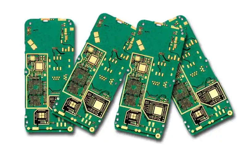
Traceability is especially important for high-reliability electronics.
A robust traceability system can connect the finished PCB or PCBA with information such as:
- Material batch
- Supplier information
- Production date
- Manufacturing process
- Equipment
- Process parameters
- Inspection results
- Test records
- Component batches
This information can help manufacturers identify the source of quality issues, conduct root-cause analysis, and implement corrective actions more efficiently.
GOPCBA’s published medical PCB capabilities emphasize documented manufacturing processes, inspection, testing, and traceability for demanding medical-electronics applications.
Designing Medical PCBs for Reliability
Manufacturing capability should be considered during PCB design rather than after the design has been completed.
Early engineering review can identify potential manufacturing problems related to:
- Minimum trace width
- Minimum spacing
- Via size
- Pad dimensions
- Layer registration
- Copper distribution
- Thermal management
- Impedance requirements
- Component spacing
- Assembly accessibility
A DFM review can help ensure that the PCB design fits within a manufacturer’s validated process window.
For advanced medical electronics, DFM and DFA analysis can also reduce unnecessary design revisions and improve production efficiency. GOPCBA provides engineering support covering DFM review, BOM verification, Gerber review, component analysis, and manufacturing feasibility evaluation.
Flexible and Rigid-Flex PCBs for Medical Electronics
Medical products are becoming smaller and more portable, creating greater demand for flexible interconnect technologies.
Flexible and rigid-flex PCBs can help reduce wiring, save space, and support three-dimensional product structures.
Potential applications include:
- Wearable medical devices
- Portable diagnostic equipment
- Compact monitoring systems
- Medical sensors
- Imaging modules
- Handheld instruments
GOPCBA supports flexible and rigid-flex PCB structures, including multilayer flexible PCBs, HDI flexible PCBs, and rigid-flex PCB assemblies.
Manufacturing for Different Medical Diagnostic Applications
Different diagnostic systems impose different PCB requirements.
CT and Medical Imaging Equipment
Imaging equipment can require high-speed signal transmission, stable power delivery, high-density interconnections, and carefully controlled electromagnetic performance.
Multilayer, high-speed, high-frequency, and controlled-impedance PCB technologies may be appropriate depending on the circuit architecture.
Ultrasound Equipment
Ultrasound systems contain signal acquisition, processing, amplification, and transducer-related circuits.
These applications can benefit from carefully controlled analog signal paths, stable power distribution, and compact multilayer PCB structures.
Laboratory and Biochemical Analyzers
Laboratory analyzers may integrate sensors, motors, pumps, heaters, optical modules, processors, and communication interfaces.
The PCB must therefore support multiple electrical functions while maintaining stable performance during repeated operating cycles.
Portable Diagnostic Devices
Portable equipment places greater emphasis on compact size, low weight, battery efficiency, mechanical durability, and efficient thermal management.
HDI, flexible, and rigid-flex PCB technologies can help engineers achieve higher integration within limited physical space.
Why Choose GOPCBA for Medical PCB Manufacturing?
Medical electronic products require a manufacturing partner capable of supporting both precision PCB fabrication and reliable assembly.
GOPCBA provides integrated PCB manufacturing and PCBA services covering prototype development, engineering review, PCB fabrication, component sourcing, SMT assembly, THT assembly, inspection, testing, and production manufacturing.
The company’s published capabilities include:
- Multilayer PCB
- HDI PCB
- High-frequency PCB
- High-speed PCB
- High-TG PCB
- Flexible PCB
- Rigid-flex PCB
- Heavy-copper PCB
- Controlled-impedance PCB
- PCB assembly
- SMT and THT assembly
- DFM engineering support
- Electrical and functional testing
This integrated manufacturing model can simplify supplier coordination and help maintain greater consistency between PCB fabrication and assembly.
For medical-electronics projects, customers can provide Gerber files, BOMs, assembly drawings, stack-up requirements, and technical specifications for engineering evaluation.
Conclusion
The manufacturing of a Medical Diagnostic PCB is a comprehensive engineering process that combines material selection, precision circuit fabrication, advanced interconnect technology, surface finishing, assembly, inspection, testing, and traceability.
As medical diagnostic equipment continues to become smaller, faster, smarter, and more integrated, PCB requirements are becoming increasingly demanding.
Multilayer construction, HDI PCB technology, controlled impedance, flexible circuits, rigid-flex structures, and advanced PCB Assembly processes can help engineers achieve the electrical performance and integration required by modern medical electronics.
The key to reliable Medical PCB Manufacturing is not one individual process. Instead, consistent quality comes from controlling every stage—from material qualification and circuit fabrication to assembly, inspection, testing, and traceability.
With integrated PCB fabrication, assembly, engineering support, and advanced manufacturing capabilities, GOPCBA provides a complete manufacturing path for medical diagnostic electronics from prototype development through production.