Multilayer PCB Lamination Process: How to Achieve Precise Layer Alignment and Void-Free Boards
The lamination process is one of the most critical stages in Multilayer PCB manufacturing. It combines inner-layer circuits, prepreg materials, copper foils, and other structural materials into a single multilayer board through controlled temperature and pressure.
During this process, two factors have a major influence on PCB quality: accurate layer alignment and the elimination of internal voids. Poor layer registration can affect circuit routing, signal integrity, via connectivity, and assembly accuracy, while internal voids can reduce mechanical strength, insulation reliability, and long-term durability.
A stable PCB Lamination Process therefore requires coordinated control of material preparation, stack-up design, alignment, temperature, pressure, resin flow, environmental conditions, and inspection.
For advanced multilayer structures, GOPCBA provides comprehensive PCB Manufacturing capabilities covering multilayer, HDI, high-frequency, high-speed, rigid-flex, controlled-impedance, and other specialized PCB technologies.
How Layer Alignment Is Controlled During Multilayer PCB Lamination
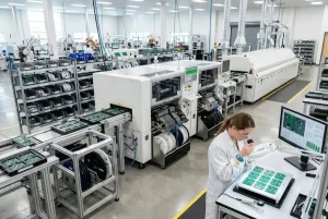
The objective of Layer Alignment is to ensure that the circuits, pads, vias, and reference features on different layers remain within the required positional tolerance after lamination.
Even a small registration error can become a significant problem when a PCB contains many layers, fine-pitch components, microvias, or controlled-impedance structures.
Material Preparation Before Lamination
The first step in achieving accurate layer registration is maintaining stable material dimensions.
After inner-layer circuit fabrication, the boards should be thoroughly cleaned to remove dust, oil, chemical residues, and other contaminants. Contamination can interfere with bonding and may create local variations between the inner layers and prepreg.
The cores, prepreg sheets, and copper foils should also be prepared according to the specified stack-up. Cutting dimensions need to be consistent, and the materials should be properly handled to avoid deformation or contamination.
Material dimensional stability is especially important for high-layer-count boards because thermal expansion can accumulate across multiple layers.
Precision Registration During Stack-Up
The stacking process determines the initial positional relationship between the individual PCB layers.
Depending on the manufacturing structure, tooling pins, registration holes, optical registration systems, or other positioning methods may be used to maintain accurate alignment.
Operators should handle the materials carefully and avoid unnecessary bending, twisting, or contamination. Fingerprints, moisture, dust, and other contaminants should be prevented from entering the stack.
Once the stack-up is completed, temporary fixation may be used to maintain the relative position of the layers before the lamination cycle begins.
For advanced HDI structures, registration becomes even more important because microvias, fine lines, small pads, and sequential buildup structures require tighter process control.
HDI PCB Design and Manufacturing Guide
Temperature and Pressure Control During PCB Lamination
Temperature and pressure directly influence both layer registration and bonding quality.
The lamination cycle should follow a controlled temperature and pressure profile rather than applying maximum pressure and temperature immediately.
Controlled Heating
During heating, the materials expand at different rates. The copper, laminate, resin, and other materials each have their own thermal characteristics.
If the temperature rises too quickly or the thermal behavior is not properly considered, differential expansion can introduce layer movement or registration errors.
A controlled heating rate allows the resin system to soften and flow progressively while reducing unnecessary mechanical stress within the stack-up.
Controlled Pressure
Pressure must also be applied in a controlled and uniform manner.
Excessive pressure at an inappropriate stage can cause material movement, resin displacement, or dimensional deformation. Insufficient pressure, on the other hand, may prevent the layers from bonding properly.
The press system must provide uniform pressure across the panel area. Equipment flatness and platen condition should therefore be regularly maintained and verified.
A stable combination of temperature, pressure, heating rate, cooling rate, and resin flow is essential for repeatable multilayer production.
How to Prevent Voids in Multilayer PCB Lamination
A Void-Free PCB structure requires effective control of air, moisture, contaminants, and volatile substances throughout the manufacturing process.
Internal voids can occur when air or gases become trapped between layers and cannot escape before the resin fully cures.
Moisture Control
PCB materials can absorb moisture during storage and handling.
When moisture is exposed to high temperatures during lamination, it can vaporize and create internal gas pockets. If the gas cannot escape, voids or delamination may occur.
For moisture-sensitive materials, appropriate pre-baking or drying procedures should be established according to the material manufacturer’s specifications.
Storage conditions should also be controlled so that materials do not absorb excessive moisture before production.
Cleanliness Control
Small particles can have a surprisingly large influence on lamination quality.
Dust, fibers, copper particles, and other contaminants can create microscopic gaps between layers. These gaps may trap air and eventually develop into internal voids.
For this reason, stacking operations should be performed in a controlled environment with clean work surfaces and appropriate handling procedures.
Operators should also use suitable protective equipment and follow standardized handling procedures.
Resin Flow and Pre-Press Conditions
Prepreg resin flow plays an important role in filling spaces between copper patterns and bonding the multilayer structure.
The lamination profile should provide sufficient time for the resin to soften, flow, and fill the required areas while allowing trapped air and volatile substances to escape.
If the resin cures too early, gases may become trapped inside the structure. If the resin flow is excessive, it can create other manufacturing problems such as resin starvation in certain areas or dimensional changes.
Therefore, resin content, prepreg selection, copper distribution, temperature, pressure, and curing conditions should be considered together.
The Importance of Lamination Stack-Up Design
A well-designed stack-up is essential for reliable multilayer PCB production.
Before manufacturing begins, engineers should evaluate:
- Number of PCB layers
- Final board thickness
- Copper thickness
- Prepreg thickness
- Core thickness
- Dielectric thickness
- Material type
- Resin content
- Signal and reference layers
- Power and ground plane distribution
- Impedance requirements
- Thermal requirements
- Via structures
- Registration requirements
For high-speed and high-frequency designs, stack-up design also directly affects impedance and signal integrity.
A properly engineered stack-up can help maintain stable dielectric dimensions, improve signal transmission, and reduce manufacturing risks.
For projects requiring complex multilayer structures, early engineering review and DFM analysis can identify potential issues before production.
Environmental Control for Stable PCB Lamination
A consistent lamination environment is another important part of process control.
Temperature and humidity fluctuations can influence material moisture content, dimensional stability, and resin behavior.
Temperature and Humidity Management
Excessive humidity can increase moisture absorption in laminate and prepreg materials, increasing the risk of voids and delamination.
Large temperature fluctuations can also influence material expansion and contraction, potentially affecting registration accuracy.
A controlled production environment therefore helps maintain more consistent material conditions before and during lamination.
Equipment Maintenance
Lamination equipment should be inspected and maintained regularly.
Important areas include:
- Press platen flatness
- Temperature uniformity
- Pressure accuracy
- Heating system performance
- Cooling system performance
- Vacuum system performance where applicable
- Tooling and registration systems
Equipment instability can directly affect lamination repeatability.
Quality Inspection After Multilayer PCB Lamination
Process control does not end when the press cycle is completed.
Finished panels should undergo appropriate inspection to verify dimensional, mechanical, and structural quality.
Depending on the PCB design and customer requirements, inspection may include:
- Visual inspection
- Dimensional inspection
- Cross-section analysis
- X-ray inspection
- Electrical testing
- Layer registration inspection
- Bonding and delamination evaluation
- Impedance testing where required
X-ray inspection can be particularly useful for identifying internal structural issues that cannot be detected through conventional visual inspection.
For PCB projects requiring both bare-board fabrication and component assembly, integrating fabrication and assembly quality control can further improve production consistency.
Common Multilayer PCB Lamination Problems
Several manufacturing problems can occur when lamination parameters are not properly controlled.
Layer Misalignment
Layer misalignment may result from inaccurate tooling, material movement, dimensional changes, improper stack-up prep
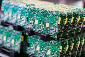
High-layer-count boards, HDI structures, fine-line routing, controlled impedance, high-frequency materials, and rigid-flex constructions all place greater demands on lamination accuracy.
GOPCBA supports advanced PCB fabrication technologies including Multilayer PCB, HDI, high-frequency, high-speed, rigid-flex, heavy copper, high-TG, metal-core, and controlled-impedance PCB manufacturing.
These capabilities allow engineers to select a PCB construction that matches the electrical, mechanical, thermal, and manufacturing requirements of the final product.
From Prototype to Production: Maintaining Lamination Consistency
Lamination parameters should remain consistent as a PCB moves from prototype development to volume production.
During prototype manufacturing, engineers can evaluate:
- Layer registration
- Board thickness
- Resin flow
- Lamination quality
- Warpage
- Electrical performance
- Mechanical fit
- Manufacturing feasibility
Once the design has been validated, production parameters can be standardized to improve repeatability.
For complex products, maintaining consistency between prototype and production is especially important because changes in materials, stack-up, equipment, or process parameters can introduce unexpected variations.
Why Choose GOPCBA for Multilayer PCB Manufacturing?
Reliable multilayer PCB production requires more than simply pressing multiple layers together. It requires coordinated engineering, material control, precision registration, controlled lamination, inspection, and manufacturing traceability.
GOPCBA provides integrated PCB fabrication and assembly services for demanding electronic applications, supporting multilayer, HDI, high-frequency, high-speed, rigid-flex, controlled-impedance, high-TG, and heavy-copper PCB technologies.
From engineering review and prototype production to volume manufacturing, the manufacturing process can be structured around the specific electrical, mechanical, thermal, and reliability requirements of each project.
For customers requiring high-density interconnect technology, GOPCBA also provides advanced HDI manufacturing capabilities including microvias, blind and buried vias, sequential lamination, and other high-density structures.
GOPCBA PCB Manufacturing Capabilities
Conclusion
A reliable PCB Lamination Process depends on the coordinated control of material preparation, stack-up design, layer registration, temperature, pressure, resin flow, environmental conditions, equipment stability, and quality inspection.
Accurate Layer Alignment helps maintain electrical connectivity and dimensional precision, while effective moisture, contamination, and gas control are essential for producing a Void-Free PCB structure.
As multilayer PCB designs become more complex, especially in HDI, high-speed, high-frequency, AI computing, automotive, telecommunications, and industrial electronics, lamination process control becomes increasingly important.
By combining disciplined engineering practices with stable materials, precision equipment, standardized processes, and comprehensive inspection, manufacturers can achieve more consistent multilayer PCB quality and improve long-term product reliability.
GOPCBA provides advanced PCB Manufacturing and PCB assembly solutions for projects ranging from prototype development to production manufacturing, helping customers build reliable and manufacturable multilayer PCB solutions.