Metal Detector PCB: Coil Drive, Phase Detection and Noise
A metal detector PCB carries an analogue instrument with a very high gain, and its design is an exercise in keeping one signal out of another. A coil is driven with a current that may be amperes, and the same coil or a second one picks up a returned signal that is a tiny fraction of the transmitted one and carries the information about what is buried. The transmitter and the receiver are separated by a factor of a million or more, and they are inches apart.
How a Detector Works Electrically
The most common arrangement is a transmit coil driven with a sinusoid and a receive coil arranged so that the transmitted field largely cancels in it. Metal near the coils changes that balance, partly by absorbing energy and partly by shifting the phase, and the receiver measures the change. Different operating frequencies suit different targets, and different coil geometries suit different ground conditions, which is why the range of products is wide.
The measurement is a vector quantity. Both the amplitude and the phase of the returned signal change with the target, and the phase shift is what allows the instrument to distinguish one kind of metal from another, or to reject the mineralisation of the soil while retaining a response to a coin.
The Transmit Drive
The transmitter is a power amplifier driving an inductive load at a frequency that may be a few kilohertz or tens of kilohertz. It must be efficient because it runs from a battery, its distortion must be low because harmonics appear in the receive band, and its current must be stable because a change in the transmitted field looks like a target.
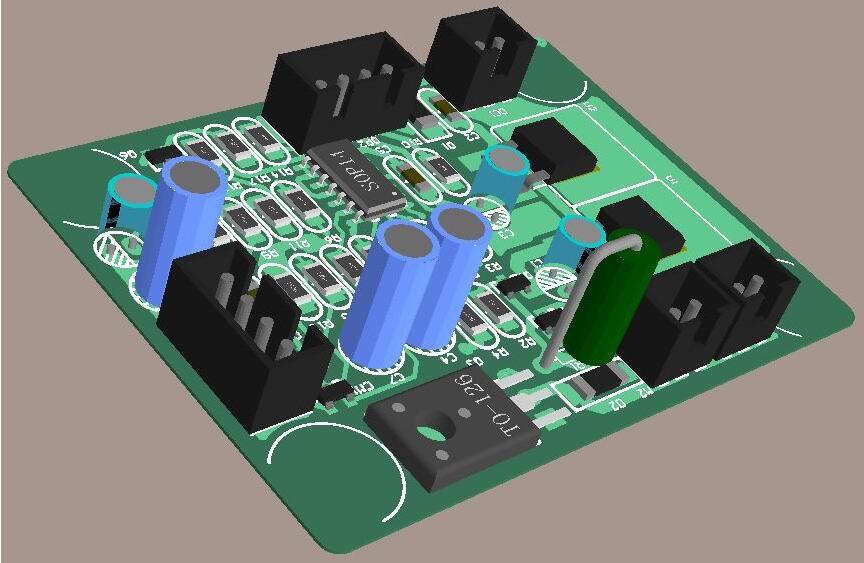
The coil current is sensed and regulated, which means the sense element is in the high current path and its signal is small compared with the drive. The layout should keep the drive loop compact, keep the sense connections Kelvin, and keep the switching devices cool, because their parameters drift with temperature and that drift appears as a change in the transmitted field. The copper that carries the coil current is sized in the usual way, as described in trace width and current calculation.
The Receive Path
The receiver begins with a low noise amplifier with a very high input impedance, and everything about that node is critical. The coil, the cable to the coil and the amplifier input form a tuned circuit whose characteristics change with temperature and with the capacitance of the cable, and the amplifier has to have enough gain that the following stages are not limited by their own noise.
The board’s contribution is leakage and pickup. A high impedance input on a contaminated surface leaks, and a receiver trace that runs near the transmit loop picks up the transmitted signal directly, which is far larger than the target response. Keeping the input traces short, guarding them, and routing the receive path so that it does not enclose the transmit field are the measures that matter. The same reasoning as in any mixed signal design applies, and it is set out in mixed signal PCB design guidelines.
Demodulation and Phase Detection
The received signal is demodulated in phase and in quadrature against the transmit reference, which yields two numbers that together describe the target. The accuracy of that comparison depends on the reference being clean and on the two channels being matched in gain and in delay, because any mismatch appears as an error in the phase angle and therefore in the identification of the target.
The board supports this by matching the two signal paths. Identical components, symmetrical routing and a shared thermal environment keep the channels aligned, and where the design allows it, the two channels are switched rather than duplicated so that a single path performs both measurements. That approach removes the mismatch at the cost of a switching arrangement that must not introduce its own error.
Ground Balance and Drift
The ground itself responds to the search field. Mineralised soil produces a signal that is many times larger than the target, and the instrument removes it by measuring its phase, which differs from that of a metal target. That means the phase reference has to be stable to a fraction of a degree, which is a requirement on the analogue chain and on its temperature behaviour.
Drift is the practical limit on sensitivity. A detector is operated for hours at a time, and a slow change in the amplifier, in the coil or in the supply appears as a false signal. Symmetry, low drift components and a thermal layout that keeps the analogue stages at a similar temperature all reduce it, and the firmware usually includes a slow tracking loop that removes what remains.
Power and Regulation
The instrument runs from a battery pack and needs several regulated rails, including a clean analogue supply for the receiver and a separate supply for the digital processing. A switching regulator is used for efficiency, but its switching frequency and its harmonics must be kept away from the operating frequency of the detector and from the narrow band around it, which is one of the few places where a linear regulator after the switcher is genuinely worth its inefficiency.
The converters should be placed away from the analogue section, with their input loops compact and their outputs filtered. The rules that govern those layouts are described in DC to DC converter layout and routing.
Layout: Separating the Two Worlds
The transmit and receive sections should occupy separate regions of the board with a defined boundary between them, and the connector that goes to the coil should be placed so that the transmit current returns by the shortest possible path. A ground plane that carries both the transmit return and the receive reference will inject the transmit current into the receiver as a voltage across the plane, which is often larger than the signal of interest.
The mitigation is to give the transmit return its own path back to the supply, and to reference the receive circuit to a point that the transmit current does not flow through. Where the two must meet, they meet at one point, near the power entry, and the arrangement follows the same reasoning as in any design where a large current and a small signal share a board.
Testing in the Field
Bench testing with a target at a fixed distance establishes that the instrument works, but it does not reproduce the conditions that matter. The detector should be tested over mineralised ground, over wet ground, and with the coil at the real distance from the electronics, because the coil cable is part of the tuned circuit and its length and position affect the result.
Temperature testing is equally important because the drift that limits sensitivity is thermal. A unit that performs well at room temperature and develops a random signal after an hour in the sun has a thermal design problem, and the layout of the analogue section and its separation from the power stages are where that problem is solved.
FAQ
Why is the receiver so sensitive to layout? Because the returned signal is a tiny fraction of the transmitted one, and any path by which the transmitter can reach the receiver directly will swamp it.
Can a switching supply be used? Yes, with filtering and a switching frequency chosen away from the operating frequency. A linear regulator afterwards makes the analogue design much easier.
What limits the depth of detection? In practice the stability of the electronics. The signal from a deep target is present, but it is smaller than the drift of the analogue chain and of the ground response.