Microstrip vs Grounded Coplanar Waveguide for RF Boards
A microstrip line and a grounded coplanar waveguide carry the same signal, but they behave differently in ways that matter once the frequency climbs into the gigahertz range. Both are quasi-TEM structures: the electric field runs between the conductor and the ground, and the wave travels along the trace. The difference is where the ground sits and how much field escapes into the substrate and into the air above it.
Choosing between the two is a question of loss budget, board area, fabrication tolerance and how much isolation the neighbouring traces need. The rules below are the ones that decide the answer in practice.
Two Ways to Guide a Wave
A microstrip line is a single conductor on the outer layer with a solid ground plane beneath it. The field is split between the substrate and the air, which makes the effective dielectric constant a weighted average of the two and pushes the structure toward dispersion as frequency rises.
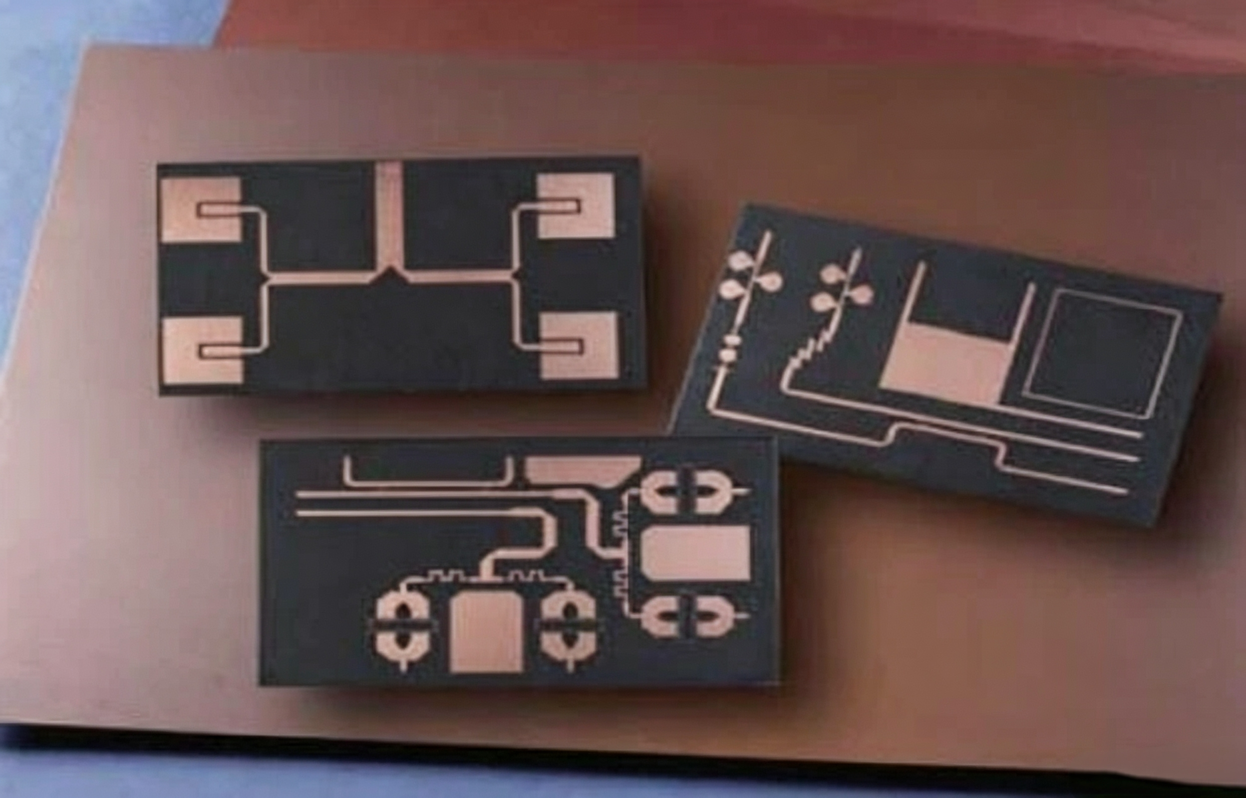
A grounded coplanar waveguide places ground copper on both sides of the trace, on the same layer, and connects that copper to the plane below with stitching vias. The field is now shared between the gaps to the side and the substrate beneath, which raises the effective capacitance and pulls the field tighter around the trace.
Impedance and Dispersion
Characteristic impedance is set by the trace width, the height to the plane, and the gap to the side ground. For a 50 ohm microstrip on 0.2 mm of FR-4 with a dielectric constant of 4.3, the trace is roughly 0.35 mm wide. For a grounded coplanar waveguide with 0.3 mm gaps, the same impedance needs a noticeably narrower trace because the side grounds add capacitance.
The practical consequence is that a grounded coplanar waveguide holds its impedance more tightly when the substrate thickness varies, because part of the field is controlled by the coplanar geometry on the same layer. A microstrip line depends entirely on the vertical distance to the plane, so a laminate thickness tolerance of ten percent becomes an impedance tolerance of several ohms.
Loss, Radiation and Isolation
At low gigahertz frequencies the two are close. As frequency rises, the grounded coplanar waveguide wins on radiation loss because the side grounds and stitching vias confine the field, while the microstrip line radiates from its edges and couples into anything parallel to it. That confinement also improves isolation between adjacent traces, which matters in dense RF PCB layout where several 50 ohm lines run side by side.
The microstrip line wins on simplicity. Its single ground plane is easy to fabricate, its performance is insensitive to the exact width of the side gaps, and the structure is mechanically robust. Because the field is only partly in the substrate, the microstrip is also less sensitive to variations in the conductor etch and in the plated copper thickness. Where several such lines run in parallel, the 3W spacing rule remains the first defence against coupling between them.
Where Fabrication Tolerance Bites
Grounded coplanar waveguide costs more to make. The narrow gaps between the trace and the side ground must be etched accurately, and a gap that comes out 20 percent wide changes the impedance more than a width error would. The stitching vias add drilling and plating steps and must be placed close enough together to keep the side grounds at the same potential as the plane.
Microstrip is forgiving by comparison, but it is not immune. Surface finish, solder mask over the trace, and the plated thickness of the copper all shift the impedance a little. Solder mask raises the effective dielectric constant above the trace and can move a 50 ohm line down by a few ohms, which is why impedance-controlled designs specify whether the mask is included in the calculation.
<img src="https://www.gopcba.com/wp-content/uploads/2026/08/pcb15.jpg" alt="Compensated transmission line bend on an RF PCB” />
The Bend Radius Rule
Any transmission line bend disturbs the current distribution. Where the line turns, the charge crowds on the inside of the corner and thins on the outside, which raises the local capacitance and produces a small discontinuity. The standard defence is a gradual bend, and the accepted rule is that the radius of the curve should be at least three times the width of the centre conductor.
Written as a formula, the bend radius is greater than or equal to three times the line width. At 0.35 mm width that means a radius of about 1 mm, which is easy to lay out. A tighter curve concentrates the discontinuity, raises the return loss at the corner, and in a differential pair also introduces a small amount of skew. Keeping the two traces symmetric through the turn, as described in the differential pair routing notes, removes most of that penalty.
Right-Angle Bends and Compensation
When the layout has no room for a gradual curve, a right-angle corner is acceptable if it is compensated. The corner behaves electrically like a short length of wider line, because the diagonal of the square corner fills the current path and increases the local capacitance. Trimming the outer corner at 45 degrees, or chamfering it, removes most of that effect and restores the impedance through the turn.
The alternative is a mitred corner done properly, where the outer edge is cut back until the electrical length through the corner matches the straight line. In practice a 45 degree chamfer whose size is about 0.5 to 0.7 times the line width is enough for most boards below 10 GHz, and the residual reflection is small enough to ignore.
Choosing Between Them
Reach for the microstrip line when the board is simple, the frequency is moderate, and cost or fabrication tolerance dominates. Reach for the grounded coplanar waveguide when the design needs tight impedance control, low radiation, or several closely spaced RF traces, and when the fabricator can hold narrow gaps.
Many boards use both. A transmitter front end may run a grounded coplanar waveguide from the amplifier to the antenna for isolation, while the control and bias lines run as microstrips. What matters is that the transition between the two structures is gradual and that the ground stitching continues through it, so the return current never has to jump across a discontinuity.
Connecting the Two Structures to the Rest of the Board
A transmission line is only as good as the components at its ends. The connector, the amplifier pad and the antenna feed all present a discontinuity, and each one has to be matched into the same impedance as the line. Place the matching components immediately at the pad, keep the stub length below one twentieth of a wavelength, and use the suppression principles that apply to the rest of the board when deciding how the RF section is shielded.
Ground continuity is the other half of the job. Every reference plane under the line must be unbroken from the source to the load, and the side grounds of a coplanar structure must be stitched to that plane at regular intervals. If the return current is forced to divert around a slot or a connector cutout, the impedance changes locally, and the resulting reflection appears as ripple in the measured insertion loss.
FAQ
Can I mix microstrip and grounded coplanar waveguide on one board? Yes, provided the transition is handled carefully. Keep the side grounds continuous across the change, maintain the same impedance on both sides, and taper the trace over a length of at least a few wavelengths. Abrupt changes cause reflections that show up as ripple in the insertion loss.
How often should stitching vias be placed? A common rule is every one tenth of a wavelength, which is about 12 mm at 2.4 GHz and 3 mm at 10 GHz. Place them along both sides of the trace and around every bend, and keep the distance from the via to the trace gap constant so the impedance does not vary along the line.
Is a wider trace always lower loss? For a fixed impedance the width and the substrate height are linked, so a wider trace usually means a thicker dielectric and a larger radiating aperture. Lower conductor loss therefore comes at the cost of more radiation and more coupling, which is why a loss budget has to include both terms.