Double-Sided Rigid-Flex PCB: Structure and Process
Products keep getting smaller while the amount of electronics inside them keeps growing, and the board has to absorb that contradiction. A double-sided rigid-flex PCB is one of the answers: it combines the flexibility of a flexible circuit with the structural rigidity of a rigid board, and it does so with routing on both sides of the flexible section. The result is a board that can be folded into an enclosure, terminated with normal components, and carry more interconnect than a single-sided alternative.
What it is
A double-sided rigid-flex PCB combines a two-layer flexible circuit with one or more rigid sections. Components can be mounted on both sides of the flexible portion, which is the difference between this construction and a single-sided flexible design, and the flexible regions connect seamlessly to the rigid areas.
Three consequences follow from the double-sided arrangement: a denser routing layout, better signal integrity because paths can be shorter and referenced to a plane, and greater mechanical strength in the flexible area than a single-layer circuit can provide.
The stackup
The construction is built from polyimide flexible layers carrying copper on both sides, rigid FR-4 sections that support the components and the mechanical interfaces, adhesive and coverlay materials that insulate and protect the conductors, and the vias, including microvias, that connect the layers.
A typical stackup runs from six to eight layers and combines several flexible and rigid regions into a single board. Because the flexible and rigid materials behave differently under heat and mechanical load, the stackup is planned as a system rather than as a flexible board with a stiffener added later.
The stackup drawing is the design. In rigid-flex construction, the mechanical behaviour of the finished product is decided by the layer arrangement rather than by the enclosure.
How the interconnect works
Copper traces run on both sides of the flexible portion and connect to vias in the rigid sections, which is how a signal travels from a component in a rigid area, through the flexible region, and into another rigid area.
The interconnect design supports features that dense boards depend on: via-in-pad for ball grid array devices, blind and buried vias for multilayer connections, and impedance-controlled routing for high-speed signals. Together, those features preserve signal integrity across the transition between the flexible and rigid regions, which is the part of the board where the geometry changes and where a design is most likely to lose margin.
Manufacturing sequence
Production begins with material preparation, combining the flexible and rigid laminates with their copper layers. Drilling and via plating follow, which is the step that creates the interconnections through the rigid sections and, where the design requires it, into the flexible regions.
The double-sided flexible layers are then imaged and etched, and the rigid and flexible sections are laminated together into a single board. Coverlay is applied to protect the flexible conductors, and a surface finish such as electroless nickel immersion gold or an organic solderability preservative is applied to the areas that will be soldered.
Electrical test and inspection complete the process. Because the construction combines two material systems, acceptance is usually defined against the applicable rigid-flex standard and a defined acceptance class, and the test plan should be agreed before the first panel is built.
Advantages
Space is the first benefit. A rigid-flex board can be folded into an enclosure that would never accept a flat board, which allows a product to be smaller without shrinking its electronics.
Reliability improves because the design uses fewer connectors: every cable and connector pair that a rigid-flex assembly replaces is a mechanical failure point that no longer exists. Dynamic flexibility is the third advantage, since a flexible section can survive movement and vibration in a way that a cable harness cannot, and the fourth is electrical, because shorter paths between rigid sections reduce electromagnetic interference rather than requiring it to be filtered out later.

Every connector removed from a design removes two contact interfaces that would otherwise need to survive the life of the product.
Applications
Aerospace electronics modules use the construction where weight and reliability are both constrained. Medical diagnostics and implantable devices use it because the board has to fit a body rather than a rack, and wearables such as smart watches and fitness bands rely on it to combine a curved enclosure with a populated board.
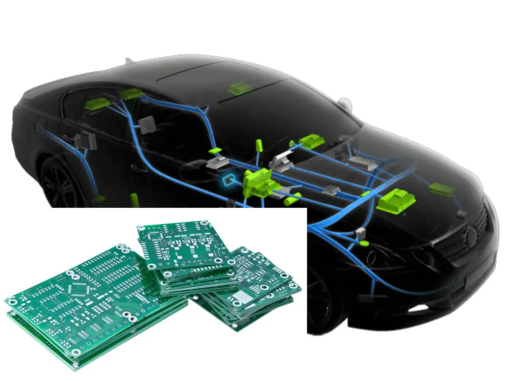
Automotive advanced driver assistance systems and infotainment modules complete the list, since both need dense electronics in a space defined by the vehicle interior, and both operate in an environment with vibration and thermal cycling.
Design considerations
Bend radius is the first constraint, and it should be treated as a material specification rather than a preference, because a bend tighter than the laminate allows will fracture the conductors. Thermal expansion is the second: the flexible and rigid materials expand at different rates, and the stackup has to accommodate that difference, as described under PCB dimensional stability and expansion.
Impedance control carries across the transition between materials, so a high-speed net should be planned as a single path rather than as two separate routings. Pad and spacing rules in the flexible area also differ from the rigid area, because the same geometry that is safe on a stiff board can crack a flexible one. Engaging the fabricator during layout is the practical answer, since a stackup review costs nothing and a re-layout costs a program.
Cost structure
Layer count and via count set the base of the cost, and the finish choice adds to it. A custom stackup with impedance control costs more than a standard construction, and the test and certification requirements of the target market add their own share. Vias that must be filled or plated in specific ways are priced accordingly, and the differences between the options are described in our guides to via in pad versus plated through and to blind and buried via stack selection.
Quantity then moves the unit price substantially. A prototype built in single digits carries the whole tooling and setup cost, while a production order spreads it across thousands of boards, which is why a prototype quotation should never be used as the basis for a production budget. For a product where reliability, space, and mechanical flexibility all matter, the higher entry cost is usually recovered by the connectors and assembly steps that the design no longer needs.
A note on the transition region
The area where the flexible section meets the rigid section deserves its own review. Conductors narrow, the material changes, and mechanical stress concentrates, so the layout should keep vias and plated features out of the transition and hold the bend well clear of it.
FAQ
How is a double-sided rigid-flex board different from a single-sided one? The flexible section carries copper on both sides, which roughly doubles the routing capacity and improves signal integrity by allowing closer reference planes, at the cost of a more involved lamination process.
How tight can the bend be? The limit comes from the laminate and the copper, not from the design intent. The fabricator should state the minimum bend radius for the specific stackup, and the design should keep the bend away from pads and vias.
Is rigid-flex worth it for a low-volume product? It can be, when the alternative is a cable harness and several connectors that would have to be assembled and tested anyway. The calculation is total assembly cost, not board cost.