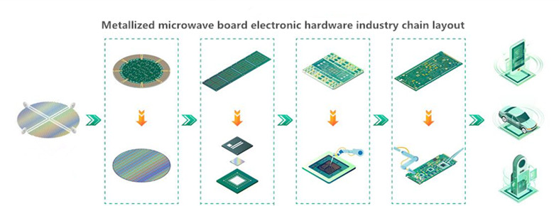
With the rapid development of science and technology, particularly information and communication technologies, the demand for advanced printed circuit boards continues to increase. Modern applications in wireless communications, transportation, radar, aerospace, automotive electronics, and other high-performance fields require circuit boards capable of handling higher frequencies, faster signal transmission, tighter impedance tolerances, and more demanding environmental conditions.
As a result, Microwave High-Frequency PCB technology has become increasingly important. Compared with conventional FR-4 circuit boards, microwave and high-frequency boards require tighter control of material properties, transmission-line geometry, copper thickness, dielectric thickness, drilling, plating, etching, and dimensional accuracy.
For PCB manufacturers such as Kingda, successfully producing a reliable High-Frequency PCB requires more than advanced equipment. It also depends on disciplined process control, experienced engineering teams, appropriate material selection, and careful inspection at every manufacturing stage.
Basic Requirements for Microwave High-Frequency PCBs
1. Material Selection and Electrical Requirements
The substrate is one of the most important factors in a Microwave PCB. During PCB design, engineers normally select the dielectric constant (Dk), dielectric thickness, copper thickness, and other material parameters according to the required characteristic impedance and operating frequency.
Unlike conventional digital PCBs, high-frequency circuits can be highly sensitive to variations in dielectric properties and transmission-line geometry. Therefore, the PCB manufacturer must carefully review the customer’s design files and confirm that the selected materials and stack-up can meet the specified electrical requirements.
Important material parameters may include:
- Dielectric constant (Dk)
- Dissipation factor (Df)
- Dielectric thickness
- Copper thickness
- Coefficient of thermal expansion (CTE)
- Thermal conductivity
- Moisture resistance
- Dimensional stability
For demanding RF and microwave applications, material selection should be evaluated together with impedance requirements, operating frequency, thermal conditions, and manufacturing capability.
2. Transmission-Line Manufacturing Accuracy
High-frequency signals are extremely sensitive to changes in transmission-line geometry. Trace width, spacing, copper thickness, dielectric thickness, and conductor shape can all affect characteristic impedance and signal attenuation.
Therefore, Impedance Control is a critical requirement for a High-Frequency Circuit Board.
Depending on the design and manufacturer capability, transmission-line width and spacing may require very tight tolerances. In precision microwave applications, tolerances around ±0.02 mm may be specified, while even tighter tolerances can be required for specialized designs.
The conductor profile should also be carefully controlled. Trace edges should remain clean and uniform, with minimal burrs, undercut, over-etching, or irregularities.
Particular attention should be paid to:
- Trace width
- Trace spacing
- Copper thickness
- Dielectric thickness
- Etch compensation
- Conductor sidewall profile
- Registration accuracy
- Impedance tolerance
Maintaining these parameters within specification is essential for consistent RF performance.
3. Plating and Copper Thickness Control
Copper plating has a direct influence on the final conductor thickness and therefore affects impedance and transmission-line geometry.
This becomes particularly important for microwave boards containing plated through-holes, vias, and other interconnection structures. Excessive or uneven plating can change conductor dimensions, while insufficient plating can reduce reliability and current-carrying capability.
For this reason, PCB Manufacturing processes must carefully control plating thickness, uniformity, current density, bath chemistry, temperature, and plating time.
A controlled copper-plating process should provide:
- Uniform copper deposition
- Consistent finished copper thickness
- Reliable via and through-hole connections
- Good adhesion
- Stable electrical performance
- Adequate mechanical reliability
For high-frequency applications, copper surface condition and conductor roughness should also be considered because conductor losses become increasingly significant as frequency increases.
4. Mechanical Processing Accuracy
Microwave laminates can behave differently from conventional epoxy/glass PCB materials during cutting, drilling, routing, and forming.
Therefore, mechanical processing requires appropriate tooling and parameters for the selected substrate.
Dimensional tolerances may commonly be around ±0.10 mm for general applications, while high-precision microwave boards may require tighter tolerances depending on the product structure and customer specifications.
The manufacturing team should consider:
- Material hardness and construction
- Thermal expansion
- Board thickness
- Tool selection
- Cutting speed
- Feed rate
- Cooling requirements
- Burr formation
- Dimensional stability
Improper mechanical processing can introduce deformation, burrs, delamination, or dimensional deviations that may ultimately affect RF performance.
Key Considerations in Microwave High-Frequency PCB Manufacturing
1. Engineering Data and CAM Processing
Engineering preparation is the foundation of high-quality PCB Manufacturing.
During CAM processing, engineers should carefully review the customer’s design data and identify critical electrical and mechanical requirements.
Two areas deserve particular attention.
First, the engineering team must understand the required transmission-line accuracy and impedance specifications.
Second, the manufacturing process must be adjusted according to the actual capabilities of the production facility. This may include etch compensation, line-width compensation, drill selection, impedance modeling, stack-up verification, and manufacturing tolerances.
Before production begins, Kingda can review the design for manufacturability and identify potential risks that may affect impedance, registration, yield, or reliability.
2. Material Cutting
Conventional PCB materials can often be processed using standard shearing or automated cutting equipment. However, microwave laminates may require different cutting methods depending on their mechanical characteristics.
Improper cutting can introduce stress, deformation, edge damage, or dimensional instability.
For certain microwave materials, CNC routing or precision cutting may provide better control than conventional shearing.
The selected method should ensure:
- Flatness
- Clean edges
- Stable dimensions
- Minimal mechanical stress
- Low risk of material damage
3. Drilling
PCB Drilling is another critical process for microwave circuit boards.
Different dielectric materials may require different drilling parameters. Drill geometry, tip angle, flute length, spindle speed, feed rate, and retract settings may need to be optimized according to the substrate.
For metal-backed or metal-core microwave materials, drilling can be particularly challenging because the structure differs significantly from conventional multilayer PCBs.
Improper drilling may result in:
- Burrs
- Hole-wall damage
- Delamination
- Resin smear
- Dimensional deviation
- Poor via reliability
Therefore, drilling parameters should be validated for each material system rather than simply applying standard FR-4 settings.
4. Through-Hole and Ground Via Processing
Ground vias are frequently used in RF and microwave PCB structures to provide low-inductance return paths and improve electromagnetic performance.
The via structure should be designed and manufactured carefully because via inductance, spacing, and connection quality can influence RF performance.
For certain specialized substrates, conventional chemical copper deposition may present additional process challenges. In these cases, alternative surface preparation and metallization methods may be considered based on the material construction.
The final via structure should provide stable electrical continuity and sufficiently low resistance while maintaining mechanical reliability.
5. Image Transfer
Image transfer is an important step in maintaining circuit geometry.
The selected photoresist, exposure system, developing process, and artwork must be capable of meeting the required line width and spacing tolerances.
For fine-line Microwave High-Frequency PCB production, exposure accuracy and registration control become increasingly important.
Engineering and production teams should verify:
- Artwork accuracy
- Exposure resolution
- Registration
- Photoresist uniformity
- Developing conditions
- Fine-line integrity
Stable image transfer provides a solid foundation for subsequent PCB Etching.
6. PCB Etching
PCB Etching directly determines the final geometry of the copper traces.
For high-frequency boards, the etching process must be tightly controlled because excessive undercut, over-etching, or uneven trace profiles can alter transmission-line dimensions and characteristic impedance.
Important process parameters include:
- Etchant concentration
- Etchant temperature
- Spray pressure
- Conveyor speed
- Copper loading
- Etch compensation
The objective is to produce clean and uniform traces with minimal burrs, notches, excessive undercut, or dimensional variation.
For precision microwave circuits, the final trace width should be verified against the design and impedance requirements.
7. Surface Finish and Plating
Microwave PCBs can use different surface finishes depending on the application, assembly method, reliability requirements, and electrical performance.
Common options include:
- Electroless nickel immersion gold (ENIG)
- Immersion gold
- Immersion silver
- HASL
- Other application-specific finishes
For many high-frequency and microwave applications, ENIG or other controlled surface finishes may be selected because they provide good solderability and environmental protection.
However, surface finish selection should not be based solely on appearance or solderability. The impact on RF loss, conductor geometry, connector interfaces, and long-term reliability should also be considered.
8. CNC Routing and Board Forming
CNC routing is commonly used for precision forming of microwave and high-frequency boards.
Different substrate constructions may require different routing tools, feed rates, spindle speeds, and cooling methods.
For metal-backed microwave boards, for example, routing parameters can differ substantially from those used for standard multilayer FR-4 boards.
Proper routing control helps prevent:
- Burrs
- Edge damage
- Delamination
- Board deformation
- Dimensional errors
- Excessive mechanical stress
Additional Quality-Control Considerations
In addition to the major processes described above, high-frequency PCB production requires careful control of the entire manufacturing chain.
Impedance Testing
Impedance should be verified using appropriate test methods and representative test coupons. The measured results should be compared with the customer’s specified impedance requirements.
Dimensional Inspection
Board thickness, outline dimensions, hole locations, trace widths, and registration should be inspected to ensure that the finished board meets drawing specifications.
Surface Inspection
Copper surfaces, solder mask, plating, and finished traces should be inspected for scratches, dents, contamination, oxidation, exposed copper, and other defects.
Thermal Process Control
Processes involving elevated temperatures, such as soldering and thermal treatment, should be controlled carefully because microwave materials can have different thermal expansion characteristics from conventional PCB materials.
Cleanliness
Contamination on RF surfaces can negatively affect solderability, reliability, and in some applications, high-frequency electrical performance. Appropriate cleaning and handling procedures should therefore be established.
Why Process Control Matters for Microwave PCBs
The performance of a microwave circuit is determined not only by its schematic and PCB layout but also by how accurately the physical board reproduces the design.
A small change in trace width, dielectric thickness, copper thickness, surface condition, or registration can affect impedance and insertion loss. At higher frequencies, these variations become increasingly important.
Therefore, producing a reliable High-Frequency PCB requires close cooperation between PCB designers, material suppliers, engineers, and manufacturing teams.
Kingda can support high-frequency and microwave PCB production through engineering review, material selection, controlled fabrication processes, impedance control, precision drilling, copper plating, etching, surface finishing, CNC routing, and final inspection.
Conclusion
The manufacturing of a Microwave High-Frequency PCB is significantly more demanding than conventional PCB production. Material properties, transmission-line geometry, copper thickness, impedance control, drilling, plating, etching, mechanical processing, and surface quality all need to be carefully controlled.
The most important principle is to treat the entire manufacturing process as an integrated system rather than focusing on a single production step. From CAM engineering and material preparation to PCB Drilling, PCB Etching, plating, surface finishing, and final inspection, every stage can influence the electrical and mechanical performance of the finished board.
With appropriate material selection, precise process control, reliable inspection, and experienced engineering support, manufacturers such as Kingda can consistently produce high-quality Microwave PCB and High-Frequency PCB products for demanding RF, communication, automotive, aerospace, and other advanced electronic applications.