Miniaturized HDI PCB for 5G Communication Modules
As communication technologies continue to evolve, 5G modules are becoming smaller, faster, and more highly integrated. This trend creates increasingly demanding requirements for circuit board design and manufacturing. Conventional PCB structures may not provide sufficient routing density or space efficiency for compact communication systems.
A Miniaturized HDI PCB provides an effective solution by integrating fine-line circuits, microvias, blind vias, buried vias, and high-density interconnections into a compact board structure. By optimizing electrical connections within a limited physical area, HDI technology allows engineers to reduce PCB size while maintaining the routing capacity and electrical performance required by modern 5G communication equipment.
For communication modules used in smartphones, industrial IoT equipment, automotive electronics, wearable devices, and other connected products, advanced HDI PCB Manufacturing technology can provide the high-density interconnection capability required for increasingly compact electronic designs.
1. Miniaturization Solves Space Constraints in 5G Devices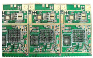
Miniaturization is one of the most important requirements for modern 5G communication modules. As electronic products become smaller and more functional, designers need to accommodate processors, memory, RF components, power-management circuits, antennas, and communication interfaces within increasingly limited spaces.
A conventional PCB often requires relatively large routing areas and through-hole structures. These limitations can make it difficult to achieve the required connection density in compact products.
A High-Density Interconnect PCB uses advanced interconnection structures to overcome these limitations. Microvias and sequential buildup technology allow electrical connections to be established between selected PCB layers without relying entirely on conventional through-holes.
This approach can reduce unnecessary routing space and improve the utilization of the available board area.
The benefits include:
- Higher routing density
- Smaller PCB dimensions
- More efficient layer utilization
- Reduced interconnection distances
- Greater flexibility for component placement
- Better suitability for compact electronic products
For 5G communication modules, these advantages are particularly valuable because the PCB must accommodate high-speed signal paths while supporting a large number of components and interfaces.
GOPCBA provides advanced PCB fabrication capabilities covering HDI, multilayer, high-speed, high-frequency, rigid-flex, controlled-impedance, and other specialized PCB technologies.
2. High-Density Interconnection Supports High-Speed 5G Signals
The higher data rates and operating frequencies associated with modern communication systems place strict requirements on signal integrity.
A 5G Communication Module PCB must maintain stable electrical characteristics throughout the signal path. Trace geometry, dielectric thickness, layer structure, via design, impedance, and material properties can all influence signal transmission performance.
By shortening interconnection paths and optimizing layer-to-layer connections, HDI technology can help engineers create more compact and controlled signal-routing structures.
The use of microvias is especially important in high-density designs. Compared with conventional through-hole vias, microvias can provide more localized connections between adjacent layers. This can free routing space and reduce the need for long vertical interconnections.
For high-speed communication applications, PCB stack-up design is also critical. Signal layers should be arranged with appropriate reference planes to provide predictable return-current paths and help control impedance.
The combination of optimized stack-up design, controlled impedance, high-density routing, and precision manufacturing provides a reliable foundation for high-speed communication modules.
GOPCBA’s PCB manufacturing capabilities include HDI, high-speed PCB, high-frequency PCB, impedance-controlled PCB, blind and buried vias, and other advanced technologies.
3. Microvias and Blind/Buried Vias Improve Routing Efficiency
One of the defining characteristics of a Miniaturized PCB is its ability to accommodate complex electrical connections within a limited physical footprint.
Microvias, blind vias, and buried vias provide engineers with greater flexibility when connecting different circuit layers.
Microvias
Microvias are typically formed using laser drilling and are significantly smaller than conventional mechanical vias. Their compact dimensions make them particularly useful for fine-line and high-density PCB structures.
In 5G modules, microvias can help connect high-density component areas while preserving valuable routing space.
Blind Vias
Blind vias connect an outer layer to one or more internal layers without passing completely through the PCB. This structure can help reduce routing congestion and improve space utilization.
Buried Vias
Buried vias are located entirely within the internal layers of a multilayer PCB. They can provide additional routing flexibility without occupying space on the external surfaces.
Combining these structures allows designers to create sophisticated interconnection architectures suitable for compact communication modules.
For advanced designs, via dimensions, aspect ratio, hole positioning, copper plating, layer registration, and via filling processes must all be carefully controlled during HDI PCB Manufacturing.
GOPCBA supports advanced PCB structures including blind vias, buried vias, microvias, and other high-density interconnection technologies.
4. Applications of Miniaturized HDI PCB Technology
The benefits of HDI technology extend across multiple industries where compact dimensions, high signal density, and reliable electrical performance are required.
5G Communication Equipment
5G base-station equipment, communication modules, RF systems, and networking hardware require high-speed signal transmission and efficient use of PCB space.
HDI structures can provide the routing density required to integrate complex communication functions into compact module architectures.
Industrial IoT
Industrial IoT sensors, gateways, controllers, and wireless communication devices increasingly require smaller form factors while supporting multiple communication protocols.
A High-Density Interconnect PCB can help integrate communication, processing, power management, and sensor interfaces within a compact electronic assembly.
Automotive Electronics
Connected vehicles and intelligent transportation systems require reliable communication between electronic control units, sensors, processors, and wireless modules.
Miniaturized HDI structures can support compact automotive communication modules while providing the routing density required for increasingly sophisticated vehicle electronics.
Consumer Electronics
Smartphones, wearable devices, tablets, portable communication equipment, and other consumer electronics continuously pursue thinner and lighter product designs.
The compact architecture of HDI technology allows more functions to be integrated into smaller PCB footprints, supporting the development of increasingly sophisticated portable devices.
Medical and Security Electronics
Medical equipment and intelligent security products may also require compact circuit boards with stable high-speed communication capabilities.
In these applications, HDI technology can help balance miniaturization, electrical performance, reliability, and manufacturing requirements.
GOPCBA provides PCB manufacturing and PCBA solutions for communications, automotive electronics, medical electronics, industrial automation, AI, IoT, and other application fields.
5. Manufacturing Challenges for Miniaturized HDI PCBs
Although HDI technology provides significant design advantages, miniaturized PCB structures also place higher demands on manufacturing precision.
Precise Layer Registration
As PCB dimensions and line spacing become smaller, even minor layer misalignment can affect trace spacing, pad geometry, microvia connections, and impedance-controlled structures.
Therefore, accurate registration is essential throughout lamination and circuit fabrication.
Laser Drilling Accuracy
Microvias require highly precise laser drilling. Hole diameter, depth, position, and consistency must remain within the specified process window.
Poor drilling control can lead to incomplete connections, excessive copper exposure, or other reliability problems.
Controlled Lamination
HDI PCBs frequently use sequential buildup structures. Each lamination cycle must maintain stable temperature, pressure, resin flow, and layer alignment.
Process variation can contribute to delamination, warpage, voids, or dimensional instability.
Copper Plating and Via Reliability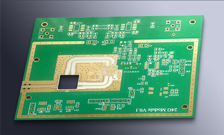
Reliable electrical connections depend on uniform copper deposition inside microvias and other plated structures.
The hole-wall condition, copper thickness, plating uniformity, and via filling process must therefore be carefully controlled.
Electrical Testing and Inspection
As routing density increases, inspection becomes increasingly important. Automated optical inspection, electrical testing, dimensional inspection, and other quality-control methods help identify potential manufacturing defects before shipment.
A reliable manufacturing process must integrate engineering review, fabrication, inspection, and testing rather than treating quality control as a final-stage activity.
6. Future Development of Miniaturized HDI PCB Technology
The development of 5G and future communication technologies will continue to increase requirements for PCB density, electrical performance, thermal management, and reliability.
Future 5G Communication Module PCB designs are likely to place greater emphasis on:
- Smaller feature sizes
- Higher interconnection density
- More advanced microvia structures
- Improved signal integrity
- Lower transmission loss
- Better thermal management
- More sophisticated multilayer architectures
- Higher manufacturing precision
As communication systems move toward higher frequencies and greater data throughput, PCB material selection will also become increasingly important.
Low-loss and high-performance laminates may be required for applications where signal attenuation and dielectric characteristics have a significant influence on system performance.
For advanced applications, HDI technology may also be combined with high-frequency materials, controlled impedance, rigid-flex construction, and high-layer-count structures to meet increasingly complex electrical and mechanical requirements.
GOPCBA supports a broad range of advanced PCB technologies, including multilayer, HDI, high-speed, high-frequency, rigid-flex, heavy copper, controlled impedance, and high-layer-count PCB manufacturing.
7. Why HDI PCB Manufacturing Capability Matters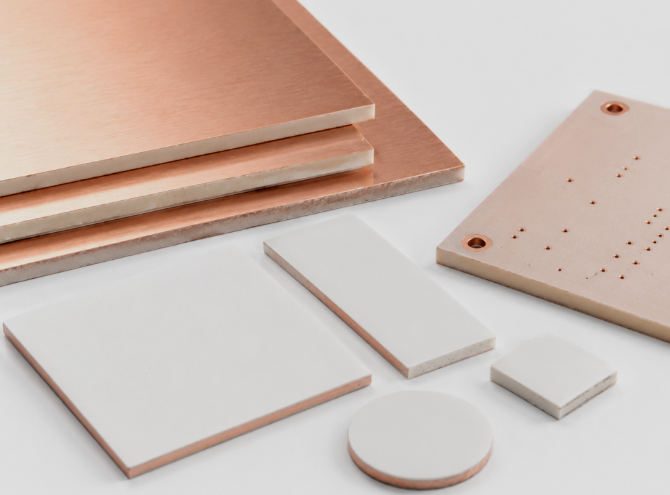
Selecting the right manufacturing partner is particularly important for miniaturized communication modules because HDI production requires close coordination between PCB design and manufacturing processes.
An experienced manufacturer should be able to evaluate:
- Layer stack-up
- Line width and spacing
- Microvia dimensions
- Blind and buried via structures
- Via filling requirements
- Material selection
- Impedance requirements
- Lamination structure
- Copper thickness
- Manufacturing tolerances
- Electrical testing requirements
Early engineering review can identify potential manufacturing risks before production begins. This can reduce design revisions, improve production yield, and help ensure that the finished PCB meets the required electrical and mechanical specifications.
GOPCBA provides PCB fabrication from prototype development through production manufacturing and supports advanced PCB requirements including HDI, multilayer, high-frequency, high-speed, and controlled-impedance structures.
Conclusion
The rapid development of 5G communication is driving electronic products toward smaller dimensions, higher integration, faster data transmission, and greater functional density. These requirements make advanced PCB technologies increasingly important.
A Miniaturized HDI PCB provides an effective solution by combining fine-line routing, microvias, blind vias, buried vias, and optimized multilayer structures. These technologies allow engineers to increase interconnection density while reducing PCB size and maintaining the electrical performance required by modern communication systems.
For manufacturers of 5G communication equipment, IoT devices, automotive electronics, consumer electronics, medical devices, and other compact electronic products, choosing an experienced HDI PCB Manufacturing partner can be critical to achieving reliable performance and consistent production quality.
With advanced fabrication capabilities and engineering support, GOPCBA provides customized PCB manufacturing and PCBA solutions for increasingly complex electronic applications.