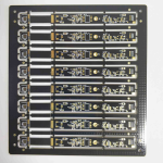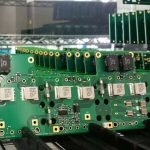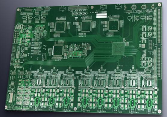
Precision 8-Layer PCB for High-Speed 5G Optical Modules
As 5G networks continue to expand across telecommunications, data centers, industrial automation, smart transportation, and other digital applications, the demand for higher data rates, lower latency, and greater transmission reliability continues to increase.
Optical modules play an essential role in converting and transmitting high-speed signals throughout modern communication infrastructure. At the same time, the PCB inside an optical module provides the electrical interconnection, signal routing, power distribution, and mechanical foundation required for stable operation.
A precision 8-layer PCB can provide an effective platform for demanding optical communication applications by combining high routing density, controlled impedance, improved signal isolation, and compact structural integration. Compared with simpler board structures, a carefully engineered multilayer design provides more routing and reference-plane options within a limited footprint.
For applications requiring advanced board structures, GOPCBA provides comprehensive PCB Manufacturing Services covering multilayer, HDI, high-frequency, rigid-flex, heavy copper, and other specialized PCB technologies.
1. Why Use an 8-Layer PCB for 5G Optical Modules?
The continuous development of 5G communication infrastructure places increasingly demanding requirements on PCB design. Optical modules must process high-speed electrical signals while maintaining stable transmission characteristics within compact mechanical structures.
An 8-layer PCB provides additional internal layers for separating signal, power, and ground functions. Instead of forcing all routing onto a small number of layers, engineers can distribute high-speed signals and power networks across an optimized stack-up.
A typical multilayer structure may include dedicated signal layers, ground reference planes, power distribution layers, and additional routing layers. The exact stack-up depends on the optical module architecture, operating frequency, impedance requirements, thermal conditions, and component configuration.
Proper layer planning can provide several advantages:
- Higher routing density
- Better signal isolation
- More controlled impedance structures
- Improved power distribution
- Reduced electromagnetic coupling
- Better utilization of limited PCB space
- Greater flexibility for high-speed circuit design
The key is not simply increasing the number of layers. The layer stack-up must be designed around the electrical and mechanical requirements of the final product.
2. High-Density Layer Stack-Up for High-Speed Signal Transmission
One of the most important characteristics of an 8-layer PCB is its ability to accommodate complex routing while maintaining controlled electrical characteristics.
High-speed optical modules can contain multiple signal channels operating at high data rates. As transmission speeds increase, trace geometry, dielectric thickness, copper characteristics, reference-plane continuity, and impedance become increasingly important.
A well-designed multilayer stack-up can place high-speed signal layers next to appropriate reference planes. This helps create predictable transmission structures and provides a controlled return path for high-speed signals.
For more demanding applications, PCB designers may also integrate HDI structures such as microvias, blind vias, buried vias, and sequential lamination. These technologies can further increase routing efficiency when component density and available board space become major constraints.
GOPCBA’s HDI PCB Manufacturing capabilities support advanced high-density interconnect structures for applications requiring compact layouts and complex interconnections.
3. Signal Integrity and Impedance Control
Signal integrity becomes increasingly important as communication systems move toward higher data rates.
In a 5G optical module, uncontrolled impedance, excessive signal loss, crosstalk, discontinuities, and poor return paths can negatively affect signal quality. Therefore, PCB manufacturing must maintain consistency between the design parameters and the physical board structure.
Important factors include:
Controlled Trace Geometry
Trace width, spacing, copper thickness, and dielectric thickness all influence impedance. Manufacturing variations must therefore be controlled within the tolerances defined by the design.
Stable Dielectric Structure
The dielectric material and its thickness affect the electrical characteristics of high-speed transmission lines. Consistent lamination and material properties help maintain predictable impedance.
Continuous Reference Planes
Ground and reference planes provide controlled return paths for high-speed signals. Proper layer arrangement can reduce unwanted coupling and improve electromagnetic performance.
Manufacturing Accuracy
Layer registration, drilling accuracy, etching consistency, plating thickness, and surface treatment can all affect the final electrical performance of a high-speed board.
For demanding RF and high-speed applications, High-Frequency PCB Manufacturing requires close control of material properties, copper geometry, dielectric thickness, impedance, and manufacturing tolerances.
4. Thermal Management in 5G Optical Module PCBs
High-speed communication equipment often operates continuously and may generate significant heat. Optical modules contain active electronic and optoelectronic components that require stable thermal conditions.
Therefore, thermal management should be considered during both PCB design and manufacturing.
A multilayer PCB can support thermal management through appropriate copper distribution, thermal vias, power-plane design, and component placement.
For example, thermal vias can transfer heat between copper layers and help distribute localized heat. Large copper areas can also improve heat spreading when appropriately integrated into the board design.
However, thermal performance should not be considered independently from signal integrity. Excessive copper changes, inappropriate via placement, or poorly designed layer transitions may affect electrical performance.
A reliable 5G optical module PCB therefore requires a balanced design approach that considers:
- Signal integrity
- Impedance control
- Power integrity
- Thermal distribution
- Mechanical structure
- Manufacturing tolerances
- Component density
The objective is to create a PCB structure that remains electrically and thermally stable during continuous operation.
5. Applications of Precision 8-Layer PCBs
Precision 8-layer PCB technology can be applied across multiple communication and electronic systems where high density, signal integrity, and reliability are important.
5G Base Stations
5G base stations require high-speed data processing and reliable communication between RF, digital, power, and optical interfaces. Multilayer PCBs can provide the routing density and electrical separation required by complex communication hardware.
For base-station applications, HDI and high-frequency technologies may be combined depending on the system architecture.
Data Centers
Data centers increasingly rely on high-speed optical interconnects to connect servers, switches, storage systems, and network equipment.
The PCB inside an optical module must support high-speed signal transmission while maintaining stable impedance and reliable electrical connections. A carefully engineered multilayer structure can provide the necessary routing density within a compact package.
Industrial Communication
Industrial networks increasingly use high-speed communication to connect controllers, sensors, machines, and remote systems.
In these environments, PCB reliability is especially important because equipment may operate continuously under temperature variation, vibration, electrical noise, and other demanding conditions.
Smart Transportation
Intelligent transportation systems require reliable communication between vehicles, roadside equipment, control systems, sensors, and network infrastructure.
High-speed multilayer PCBs can provide the compact and reliable electrical infrastructure required for communication modules used in these systems.
6. Manufacturing Considerations for 8-Layer PCBs
Producing an 8-layer PCB requires much tighter process control than a basic single- or double-sided board.
The manufacturing process generally includes inner-layer fabrication, lamination, drilling, copper plating, outer-layer imaging, etching, solder mask application, surface finishing, electrical testing, and final inspection.
Each stage can affect the final dimensional and electrical characteristics of the board.
Layer Registration
Accurate alignment between internal and external layers is essential. Registration errors can affect vias, pads, traces, and impedance structures.
Lamination Control
Lamination determines the final relationship between copper layers and dielectric materials. Pressure, temperature, curing conditions, and material properties must be controlled carefully.
Drilling and Via Quality
Through-holes, blind vias, buried vias, and microvias must meet the design requirements. Poor drilling accuracy or unreliable plating can affect both electrical performance and long-term reliability.
Copper Plating
Consistent copper deposition is important for via reliability, current carrying capability, and overall PCB durability.
Surface Finish
The appropriate surface finish should be selected according to assembly requirements, solderability, reliability, and application conditions.
Electrical Testing
Electrical testing helps identify opens, shorts, and other potential defects before shipment.
For complex multilayer boards, manufacturing quality should be evaluated across the entire process rather than at the final inspection stage alone.
7. Material Selection for High-Speed Multilayer PCBs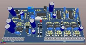
Material selection is another important consideration when developing a 5G optical module PCB.
Standard FR-4 materials may be suitable for many applications, but higher-speed designs can require materials with more stable dielectric characteristics and lower signal loss.
Material selection should consider:
- Operating frequency
- Dielectric constant
- Dissipation factor
- Thermal performance
- Z-axis expansion
- Moisture resistance
- Mechanical reliability
- Lamination compatibility
- Cost and availability
The correct material should be selected according to the actual electrical and environmental requirements rather than simply choosing the most advanced material available.
For detailed material-selection considerations, see the Multilayer PCB Material Selection Guide.
8. From Prototype to Mass Production
The requirements of an optical communication PCB can change significantly between prototype development and volume production.
During the prototype stage, engineers need to verify:
- Layer stack-up
- Signal integrity
- Impedance
- Thermal performance
- Component placement
- Mechanical compatibility
- Manufacturing feasibility
Once the design is validated, production requires stable process control and repeatable manufacturing performance.
Engineering review before production can help identify potential issues related to trace geometry, vias, layer transitions, material selection, tolerances, and assembly.
For projects requiring both bare-board fabrication and component assembly, a combined manufacturing approach can simplify supplier management and improve communication between engineering and production teams. GOPCBA also supports PCB Assembly Services for rigid, flexible, rigid-flex, multilayer, HDI, high-frequency, and other PCB types.
9. Future Development of 5G Optical Module PCBs
As communication networks continue evolving toward higher bandwidth and lower latency, PCB technology will also need to advance.
Future optical module PCBs are likely to place greater emphasis on:
- Higher transmission speeds
- More compact form factors
- Greater routing density
- Lower signal loss
- Better thermal management
- More precise impedance control
- Advanced materials
- HDI and microvia structures
- Improved manufacturing consistency
The evolution toward 5.5G and future 6G communication technologies may further increase the electrical and manufacturing requirements placed on optical module PCBs.
At the same time, manufacturers will need to balance performance, reliability, manufacturability, and cost.
Conclusion
The 8-layer PCB provides a practical multilayer platform for high-speed 5G optical modules that require high routing density, controlled impedance, signal integrity, thermal management, and compact integration.
Its value comes not simply from having eight copper layers, but from the engineering of the complete PCB structure. Layer stack-up, material selection, trace geometry, reference planes, vias, lamination, copper plating, surface finish, and electrical testing must work together to achieve consistent performance.
As communication infrastructure continues moving toward higher speeds and greater integration, precision multilayer PCB technology will remain an important foundation for optical modules, data centers, base stations, industrial communication equipment, and other high-performance electronic systems.