
Mixed-Signal PCB Layout Partitioning Rules
Mixed-signal boards fail for a predictable reason: an analog front end and a digital core share one copper plane without a floor plan. The schematic is correct, the netlist is correct, and the board still picks up noise because return currents from the digital section flow under the analog front end. The fix is not a single clever trick but a sequence of decisions made in the right order, starting before the first component is placed.
Define the regions on paper first
The first step is to divide the schematic into functional blocks: digital, analog, and the interface section that connects the board to the outside world. Inside each block, separate pure digital devices from pure analog devices and identify the mixed-signal parts, such as converters and transceivers, that belong to both. At the same time, note where the supply pins and the signal pins sit on each package, because pin location on the die determines which direction the device naturally faces.
Only then should the board outline be divided. A common starting ratio is roughly two parts digital, one part analog, and one part interface, adjusted to the actual component count. High-speed digital traces should be kept short inside the digital region, sensitive analog traces kept short inside the analog region, and supply or critical signals routed with wider copper. Devices and their traces should stay inside their assigned region rather than taking shortcuts across it.
A board that carries a telephone or line interface needs an extra caution. When that section occupies a large share of the area, control and status signals will cross it. In that case the spacing between components, the suppression of high voltage, and current limiting have to be set deliberately instead of inherited from a default rule.
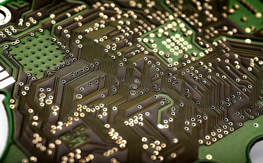
The floor plan is a commitment, not a sketch. Once the regions are drawn, every later placement decision should be checked against them.
Place the connectors before anything else
Placement starts at the board edge. Connectors and jacks define where power, ground, and signals enter the board, so their position fixes the reference for everything that follows. Leave clearance around each connector for the mating plug, and leave routing space on the board side for the supply and return paths that must reach it. Sockets deserve the same treatment: reserve the footprint of whatever will eventually be plugged into them, so a later change does not force a re-layout.
Put mixed-signal devices on the boundary
Converters, transceivers, and similar mixed-signal parts are placed next, because they physically join the two regions. Decide the orientation before the position: the digital pins should face the digital region and the analog pins should face the analog region, so that no pin has to cross the board to reach its own territory. The package then sits on the seam between the regions instead of inside either one.
Analog components come next
Analog devices are kept close to one another and placed on the side of the board where the sensitive traces run. Keep switching supplies, clock drivers, and other noisy parts away from those traces. Interface receivers and drivers belong near the connector and away from high-frequency clocks, so that noise margin comes from placement rather than from adding a choke coil and a capacitor to every line. That last point is where a large share of the cost of a noisy interface is created or avoided.
Digital components and decoupling
Digital devices are clustered to shorten trace length, and every supply pin gets a 0.1 uF decoupling capacitor connected between power and ground with the shortest traces the layout allows. That loop area is what radiates, so the capacitor is only as effective as its return path. Devices that drive a parallel bus sit close to the connector edge so the total bus length stays inside the limit set by the interface standard; a classic example is a bus specified with a 2.5 in maximum trace length. A crystal oscillator belongs next to the device it clocks, never across the board.
Tie the ground regions together on purpose
Digital ground, analog ground, and chassis earth are separated on the schematic and rejoined at one or more defined points. A 0 ohm resistor or a ferrite bead is the usual link. Choose the link location where crossings between the regions are densest and the circulating area is smallest, so that return current has the shortest path back to its source. More detail on return paths is available in our guide to ground routing and power trace planning.
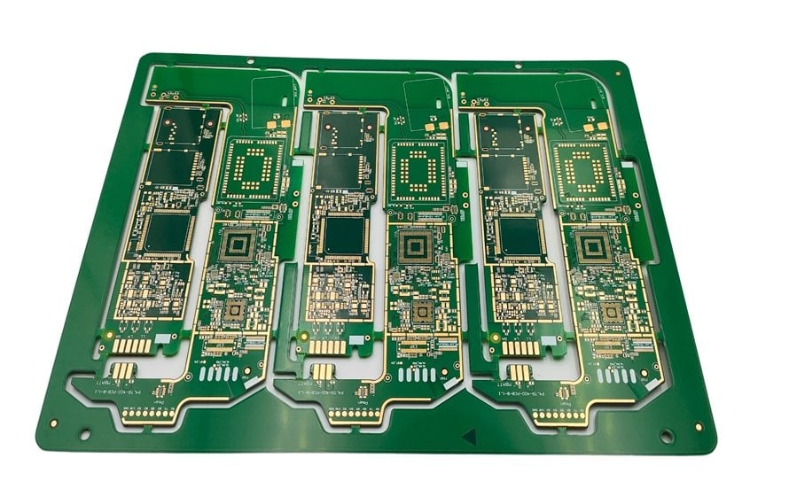
Ferrite beads are not a universal substitute for a resistor. They filter at high frequency, which helps some interfaces and hurts others, and their impedance shifts with current. The purpose of the link is to control where return current crosses between regions, so its position should come from the geometry of the board rather than from habit.
Check the plan before routing starts
Before a single trace is drawn, the placement should be annotated back into the schematic so the document and the board agree. A quick simulation at this stage is cheap and catches impedance and topology mistakes while they are still easy to fix. A short review checklist pays for itself here: does every device sit inside its assigned region, does every bypass capacitor have a short return path, and are the clock sources isolated from the sensitive analog traces?
Crosstalk is the next item to check. A trace that runs parallel to a sensitive one for a few millimetres is a capacitor, and spacing is the cheapest tool against it. The rules behind that check, and the geometry that makes them work on a real stackup, are covered in the 3W rule for crosstalk, while the broader set of partitioning decisions is set out in our mixed-signal design guidelines.
Reading the rules as one method
Every rule above answers a question that appears during a layout review: which region does this device belong to, how far may this trace run, and where does its return current go. Read as one method rather than as isolated tips, they make a mixed-signal PCB layout predictable instead of lucky. Component placement is the step where the method is either applied or abandoned, because the routing that follows can only work with the space that placement provides. A board that respects its regions, keeps the converters on the seam, and links the grounds at a deliberate point passes its bench tests and its emissions tests with far fewer iterations.
FAQ
How much area should each region take? Start from the component count and the trace density rather than from a fixed ratio. A two-to-one-to-one split between digital, analog, and interface is a reasonable first estimate, but the final split is whatever gives every trace a short path inside its own region.
Should the ground plane be split? Split it only if the layout keeps each region pure. If digital traces cross the analog area, a split plane forces return current into a long detour and the noise gets worse. A continuous plane with controlled crossings is usually the better answer.
Where does a mixed-signal device connect its grounds? The analog pins of a converter reference the analog ground and the digital interface pins reference the digital ground. That is exactly why the package sits on the boundary: the two reference systems meet at the device under controlled conditions.