What Is a Multilayer PCB?
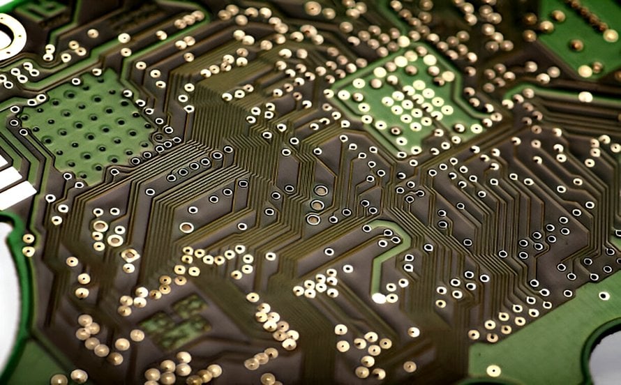
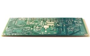
A Multilayer PCB is a printed circuit board containing three or more conductive copper layers separated by insulating dielectric materials. Unlike single-sided or double-sided PCBs, which use one or two copper layers, multilayer boards integrate multiple signal, power, and ground layers into a compact structure.
Most standard multilayer PCBs commonly use four to eighteen copper layers, while specialized boards for advanced applications can contain significantly more layers. The actual layer count depends on circuit complexity, routing density, signal integrity requirements, power distribution, mechanical dimensions, and manufacturing capabilities.
A typical multilayer PCB includes top and bottom outer layers as well as multiple internal layers. Components such as SMD and through-hole devices can be mounted on the outer layers, while internal layers are primarily used for signal routing, power distribution, and ground planes.
The different layers are electrically interconnected through Through Hole Via, Blind Via, Buried Via, and, in advanced HDI structures, microvias. These interconnection technologies allow designers to route complex circuits within a relatively small board area.
The basic multilayer PCB stackup consists of copper layers, dielectric cores, and prepreg materials laminated together under controlled temperature and pressure. The stackup must be carefully designed to achieve the required impedance, signal integrity, power integrity, thermal performance, and mechanical reliability.
Main Components of a Multilayer PCB
A multilayer PCB is made up of several functional materials and structural layers. Each plays an important role in the electrical and mechanical performance of the finished board.
Copper Layers
Copper is the primary conductive material used in a multilayer PCB. Copper layers form signal traces, power planes, ground planes, pads, and other conductive structures.
The thickness of the copper is selected according to current-carrying requirements, thermal performance, circuit density, and manufacturing specifications. High-current applications may require heavier copper, while high-density designs often use thinner copper to achieve finer traces and spacing.
Core Material
The core is a rigid dielectric material with copper foil laminated to one or both sides. It forms a stable foundation within the PCB Stackup.
FR-4 is widely used for general-purpose multilayer boards, while high-speed, high-frequency, low-loss, high-Tg, and other specialized materials may be selected according to application requirements.
Prepreg
Prepreg is a resin-based dielectric material used to bond individual PCB layers during lamination.
When heated and pressed, the resin flows and cures, creating a solid insulating structure between copper layers. Prepreg thickness and resin content are important because they affect the final board thickness, dielectric spacing, impedance, and overall stackup characteristics.
Solder Mask
The solder mask is a protective polymer coating applied primarily to the outer copper surfaces. It helps protect exposed circuitry from oxidation, contamination, and accidental solder bridging while defining the areas where components can be soldered.
Surface Finish
A surface finish is applied to exposed copper pads to improve solderability and protect the copper from oxidation.
Common finishes include HASL, ENIG, ENEPIG, immersion tin, immersion silver, and OSP. The appropriate finish depends on component requirements, assembly process, storage conditions, reliability requirements, and cost.
Vias
Vias are plated holes or micro-scale interconnections used to electrically connect different conductive layers.
Depending on their structure and depth, vias can be classified as Through Hole Via, Blind Via, Buried Via, and microvias. Via selection has a direct impact on routing density, manufacturability, reliability, and PCB cost.
Different Types of Vias in Multilayer PCBs
Vias are essential for establishing electrical connections between different layers of a multilayer PCB. The most common types include the following.
1. Through-Hole Vias
A through-hole via extends from the top surface of the PCB to the bottom surface and can connect multiple copper layers along its path.
This is one of the most common and cost-effective interconnection methods. However, through-hole vias occupy routing space on every layer they pass through, which can become a limitation in high-density designs.
2. Blind Vias
A blind via connects an outer layer to one or more internal layers without extending completely through the PCB.
Blind vias can free up routing space on internal layers and are particularly useful when greater routing density is required.
3. Buried Vias
A buried via connects internal copper layers but does not extend to either outer surface of the PCB.
Because buried vias remain inside the board, they can provide additional routing flexibility without consuming space on the outer layers.
However, their manufacturing process is more complicated than conventional through-hole vias and may increase production cost.
4. Stacked Vias
Stacked vias are vertically aligned vias placed directly above one another across multiple layers.
They are commonly used in HDI structures where space is limited. Depending on the design and manufacturing process, stacked microvias may require reliable via filling and careful control of the lamination process.
5. Staggered Vias
Staggered vias are offset from one another rather than being positioned directly on the same vertical axis.
This structure is frequently used in HDI PCB designs because it can simplify manufacturing and improve interconnection reliability compared with certain stacked-via configurations.
6. Microvias
A microvia is a very small-diameter blind or buried interconnection generally formed using laser drilling.
The commonly referenced IPC definition uses a finished hole of 0.15 mm or less for a microvia. Microvias are widely used in HDI PCB designs to achieve fine-pitch component routing and higher interconnection density.
Microvias can also be arranged as stacked or staggered structures depending on the HDI design and manufacturing process.
Advantages of Multilayer PCBs
The primary advantage of a Multilayer PCB is its ability to integrate more electrical functions into a smaller physical area.
As electronic products become smaller while their functionality and processing requirements increase, multilayer PCB technology provides designers with additional routing layers without significantly increasing board size.
1. Smaller PCB Size
Multiple internal layers allow designers to route more signals within the same board area.
Instead of expanding the PCB horizontally, additional copper layers can be added vertically. This makes multilayer construction particularly useful for compact electronic products.
2. Higher Component and Routing Density
A multilayer structure provides additional routing resources, allowing more components and connections to be integrated into a limited space.
This is particularly important for processors, communication equipment, industrial controllers, automotive electronics, and other systems with complex electrical architectures.
3. Better Signal Integrity
A properly designed PCB Stackup can place high-speed signal layers adjacent to continuous reference planes.
This reduces return-path discontinuities, limits electromagnetic radiation, and helps control characteristic impedance.
For high-speed designs, stackup planning should therefore be performed together with signal integrity analysis rather than treated as a purely mechanical arrangement.
4. Improved Power Distribution
Dedicated power and ground planes can provide low-impedance current-return paths and improve power distribution across the PCB.
A well-designed multilayer power structure can also help reduce power noise and improve overall power integrity.
5. Better Electromagnetic Performance
Ground planes and carefully arranged signal layers can reduce unwanted coupling and electromagnetic interference.
Layer arrangement, reference planes, trace geometry, via transitions, and return-current paths should all be considered during Multilayer PCB Design.
6. Greater Mechanical Stability
The laminated multilayer structure creates a rigid and mechanically stable PCB.
A properly balanced stackup can also help reduce board warpage and dimensional instability during manufacturing and assembly.
Disadvantages of Multilayer PCBs
Although multilayer PCBs provide significant design advantages, they are more demanding to manufacture than simple single- and double-sided boards.
1. More Complex Manufacturing
Multilayer PCB Manufacturing requires multiple process stages, including inner-layer fabrication, layer registration, lamination, drilling, copper plating, outer-layer imaging, solder mask application, surface finishing, electrical testing, and final inspection.
Advanced structures such as blind vias, buried vias, microvias, via filling, sequential lamination, and back drilling introduce additional process requirements.
2. Higher Manufacturing Cost
Multilayer PCBs generally cost more than simple single- or double-sided boards because they require more materials, processing steps, inspection, equipment, and manufacturing controls.
The cost can increase further when the design requires high layer counts, fine lines and spaces, HDI technology, heavy copper, special materials, controlled impedance, or advanced surface finishes.
3. Longer Production Lead Time
The additional manufacturing processes can increase production lead time.
However, actual lead time depends on the manufacturer’s equipment, capacity, production planning, material availability, board complexity, and quality requirements. An experienced manufacturer with appropriate production capacity can significantly reduce unnecessary delays.
4. More Difficult Design and Troubleshooting
As layer count increases, PCB designers must manage more complex relationships between signal layers, power planes, ground planes, vias, impedance, thermal requirements, and manufacturing tolerances.
A design problem discovered after lamination can also be more difficult and expensive to correct than an issue found during the early design stage.
Multilayer PCB Manufacturing Process
The exact Multilayer PCB Manufacturing process varies according to the board structure and manufacturing technology. A typical production flow includes the following stages.
1. DFM and Engineering Review
Before production begins, engineers review the PCB design data to identify potential manufacturing issues.
The DFM review may evaluate line width and spacing, annular rings, drill sizes, layer registration, copper distribution, impedance requirements, board thickness, stackup, solder mask, surface finish, and other manufacturing parameters.
Early DFM analysis can reduce manufacturing risks and prevent costly revisions later in the production process.
2. Material Selection and Cutting
Materials are selected according to the customer’s design requirements.
These may include copper-clad laminates, prepreg, copper foil, high-Tg materials, low-loss materials, halogen-free materials, or other specialized laminates.
The selected materials are then cut to the required production-panel dimensions.
3. Inner-Layer Fabrication
The inner copper layers are cleaned and prepared before circuit imaging.
A dry film is applied, and the circuit pattern is transferred onto the copper surface through photolithography or a related imaging process.
The unwanted copper is then removed during etching, leaving the required signal traces and planes.
4. Inner-Layer AOI
Automated Optical Inspection (AOI) compares the manufactured inner-layer pattern with the original design data.
It can identify defects such as missing traces, unwanted copper, shorts, opens, and pattern deviations.
Inspecting the inner layers before lamination is particularly important because defects hidden inside a finished multilayer board are much more difficult to identify and repair.
5. Lay-Up and Lamination
The prepared inner layers, core materials, copper foil, and prepreg are arranged according to the specified PCB Stackup.
The layer structure is then laminated under controlled temperature, pressure, and time.
During lamination, the prepreg resin melts and flows before curing, bonding the different materials into a single solid PCB panel.
Accurate layer alignment is critical during this process, especially for high-density and fine-pitch designs.
6. Drilling
After lamination, holes are drilled according to the PCB fabrication data.
Depending on the design, drilling may include through holes, blind vias, buried vias, and mechanical or laser-drilled microvias.
Drill accuracy and hole-wall quality are important because they directly affect plating reliability and electrical connectivity.
7. Copper Plating
After drilling, the exposed hole walls are prepared and metallized.
An electroless copper process establishes an initial conductive layer, followed by electrolytic copper plating to increase copper thickness.
This process creates reliable electrical connections between the different PCB layers through the drilled holes and vias.
8. Outer-Layer Fabrication
The outer copper layers are then imaged, plated, and etched according to the PCB design.
The process must maintain accurate line width, spacing, registration, copper thickness, and annular-ring dimensions.
For high-density boards, these parameters are closely controlled to ensure reliable component assembly and electrical performance.
9. Solder Mask and Silkscreen
A solder mask is applied to the outer surfaces of the PCB, leaving component pads and other designated areas exposed.
Silkscreen or legend printing may then be applied to identify component references, polarity indicators, part numbers, logos, and other assembly information.
10. Surface Finish
The exposed copper pads receive the specified surface finish.
Depending on the application, options may include ENIG, ENEPIG, HASL, OSP, immersion silver, or immersion tin.
The surface finish should be selected according to component pitch, soldering process, reliability requirements, storage conditions, and budget.
11. Electrical Testing
Electrical testing verifies the connectivity of the finished PCB.
Depending on the board design and production volume, manufacturers may use flying-probe testing, fixture-based testing, or other electrical test methods.
The test can identify potential opens, shorts, and other electrical connectivity problems.
12. Routing and V-Scoring
The finished PCB panel is separated into individual boards using routing, V-scoring, punching, or a combination of methods.
The appropriate depanelization method depends on board geometry, thickness, material, component requirements, and assembly process.
13. Final Inspection and Packaging
The completed PCBs undergo final inspection to verify appearance, dimensions, surface finish, solder mask, markings, and other specified quality requirements.
After passing inspection, the boards are packaged using suitable protective materials to minimize the risk of moisture, contamination, oxidation, mechanical damage, and electrostatic exposure during transportation.
Multilayer PCB Design Considerations
A successful Multilayer PCB Design begins with a carefully planned layer structure.
Stackup Design
The stackup should be designed according to signal speed, impedance requirements, power distribution, board thickness, material properties, and manufacturing capability.
For high-speed circuits, signal layers should generally have a controlled relationship with their reference planes to provide a predictable return-current path.
Impedance Control
High-speed and RF designs may require controlled impedance for single-ended and differential signals.
Trace width, copper thickness, dielectric thickness, dielectric constant, and reference-plane spacing all influence impedance.
Therefore, impedance requirements should be incorporated into the stackup before routing begins.
Power and Ground Planes
Continuous power and ground structures can improve current distribution and provide stable signal reference planes.
Designers should avoid unnecessary plane splits beneath high-speed signal traces because discontinuities in the return path can increase noise, radiation, and signal-integrity problems.
Via Optimization
Via placement and structure can significantly affect routing density and high-speed performance.
Through-hole vias are economical, but they occupy space across multiple layers. Blind vias, buried vias, and microvias can provide greater routing flexibility when the design justifies their additional manufacturing cost.
Thermal Management
High-power components can generate significant heat inside multilayer PCBs.
Thermal vias, copper planes, heavier copper, heat sinks, metal-core structures, and appropriate component placement can be considered according to the thermal requirements of the application.
Applications of Multilayer PCBs
Multilayer PCB technology is widely used in electronic products that require high circuit density, multiple electrical functions, and reliable signal and power distribution.
Common applications include:
- Consumer electronics: Smartphones, computers, tablets, gaming devices, and other compact products.
- Automotive electronics: ADAS systems, infotainment, ECU systems, battery management systems, and electric vehicle electronics.
- Telecommunications: Routers, switches, communication modules, base stations, and networking equipment.
- Industrial automation: PLCs, motor controllers, industrial computers, sensors, and control systems.
- Medical electronics: Diagnostic equipment, monitoring systems, imaging equipment, and portable medical devices.
- Aerospace and defense electronics: Avionics, communication systems, navigation equipment, and other high-reliability electronic systems.
- Power electronics: Power supplies, converters, inverters, and control systems.
- IoT devices: Gateways, smart sensors, connected control systems, and edge computing equipment.
Why Choose Kingda for Multilayer PCB Manufacturing?
Compared with single- and double-sided boards, multilayer PCBs require greater control over materials, layer registration, lamination, drilling, plating, impedance, and inspection.
Choosing a capable Multilayer PCB Manufacturing partner is therefore esse
chieving consistent quality and reliable production results.
Kingda can support multilayer PCB projects according to different electrical, mechanical, thermal, and manufacturing requirements. During the engineering and production process, key factors such as PCB stackup, material selection, layer count, copper thickness, via technology, impedance control, surface finish, and testing requirements can be evaluated before production.
Key advantages include:
- Professional multilayer PCB manufacturing capabilities
- Engineering and DFM support
- Flexible layer-count and material options
- Strict quality control throughout production
- Support for high-density and high-speed PCB designs
- Reliable delivery and production management
- Customized solutions based on customer requirements
For complex multilayer PCB projects, working with an experienced manufacturer from the early design stage can help identify manufacturability risks, optimize the PCB Stackup, control production costs, and improve overall product reliability.
Conclusion
A Multilayer PCB provides an effective solution for modern electronic products that require high circuit density, compact dimensions, complex routing, and reliable electrical performance.
Its combination of multiple copper layers, dielectric materials, power and ground planes, and advanced via structures enables engineers to integrate increasingly complex functions into smaller electronic devices.
However, multilayer PCB technology also requires careful design and manufacturing control. Stackup configuration, material selection, impedance, signal integrity, thermal management, via technology, lamination, drilling, plating, and inspection must all be considered together.
By selecting the appropriate structure and working with an experienced manufacturing partner such as Kingda, designers can achieve a better balance between performance, reliability, manufacturability, and cost.