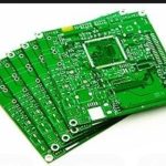
Optical Imaging PCB Solutions: Camera, LiDAR and Fiber Modules
Boards That See and Send Light
Smartphone cameras, automotive LiDAR and fiber-optic modules are pushing toward higher speed, smaller size and greater integration, and the PCB inside each one has become the foundation that makes it possible. Whether the task is high-speed data from an image sensor, precise interconnection with a photodiode, or removing heat from a laser driver, an optical imaging pcb decides performance, stability and service life. This guide examines PCB solutions across optical imaging equipment, explains the engineering requirements, materials and costs, and helps hardware teams choose the right manufacturing route for cameras, LiDAR and fiber modules.
Why the PCB Is Critical in Optical Systems
Optical systems put unusual demands on the circuit board. The PCB supports the CMOS or CCD sensor and processes its high-speed data, powers laser emitters, photodiodes and lens modules with clean, stable rails, preserves signal integrity and electromagnetic compatibility in a tiny space, manages the heat of image processors and VCSEL lasers, and enables the compact stacked constructions used in phone camera modules. As sensors gain resolution and frame rates climb, the data path from pixel to processor behaves like a high-speed communications link, which is why board material, impedance and layer structure matter as much as the optical design itself.
Signal Integrity for High-Speed Photonics
The electrical heart of an optical imaging pcb is controlled-impedance routing. Sensor and SerDes links need matched differential pairs, low-crosstalk spacing, stable power and ground planes, and short, direct paths between the sensor and its processor. For fiber modules that push tens of gigabits per second, the board must support high-speed transceivers with strict impedance tolerance and low insertion loss. In LiDAR, the return-signal processing chain runs at high speed while high-power laser drivers switch nearby, so layout discipline separates noisy drive stages from sensitive receive paths. These are board-design problems as much as circuit-design problems, and they are solved with stack-up engineering and careful routing before fabrication.

Thermal Management in Optical Modules
Heat is concentrated in exactly the wrong places in optical modules. Image processors draw real power under sustained capture, VCSEL laser arrays for LiDAR and 3D sensing generate serious heat in a small spot, and high-speed optical communication ICs run hot while their wavelength stability depends on temperature. The answers are metal-base MCPCBs where heat flux is highest, ceramic PCBs for extreme cases, and generous thermal via arrays that pull heat from the die pad to the board backside. A LiDAR emitter board that cannot shed heat will drift in power and eventually shorten its own life, so thermal design is a reliability specification, not a convenience.
Materials: Matching Loss and Frequency
Material selection follows the data rate and environment. Camera modules commonly use FR-4 or polyimide flex where space and folding matter, keeping cost low. LiDAR boards that process high-frequency signals use Rogers 4350B, Isola 370HR or similar low-loss laminates for stable dielectric performance and reliability. Fiber-optic modules need ultra-low-loss materials such as Rogers 3003 or Megtron 6 to keep high-speed signals clean across the module. Low-loss materials cost more, but they are the difference between a module that passes eye-diagram tests and one that fails them, which is why optical programs budget for material quality from the start.
Camera Module PCB Design Essentials
Camera boards concentrate several disciplines in a few square centimeters. CMOS and CCD layout shortens the signal chain, keeps a solid ground plane beneath the sensor, and limits temperature drift that shifts dark current. EMI control uses shield cans, grounded via fences around sensitive areas, and differential routing for MIPI or LVDS lanes. Autofocus and zoom systems add flexible PCBs that drive the lens motor and connect the sensor inside folded camera stacks. The result is a dense mixed construction where rigid substrate, flex circuits and connectors must align to tenths of a millimeter.

LiDAR System Boards
LiDAR electronics split into two worlds on the same system. High-power laser driver boards need 1-3 oz copper, wide current paths and serious heat spreading to switch the emitter safely. Signal-processing boards for the return path use eight to twenty layers of HDI with low-loss material and BGA-compatible routing for the processing silicon. Automotive-grade reliability wraps around both: high-temperature tolerance, vibration survival and humidity and corrosion resistance for modules mounted on vehicles. For autonomous-driving programs, the PCB failure mode is not an inconvenience but a safety issue, so Class 3 manufacturing and automotive qualification are the norm.
Fiber Optic Module Boards
Optical transceivers such as SFP, QSFP and GPON modules are high-speed boards in miniature. They need very high bandwidth, strict impedance control and SerDes-compatible design at the module edge connector, plus precisely placed pads for the laser and photodiode that are aligned during assembly. Power delivery must be extremely low noise because laser bias circuits amplify every microvolt of ripple. Materials such as Megtron 6 and Rogers families give the stable Dk and low loss that 25G, 50G and faster lanes require, and the assembly process must handle optical components and high-speed connectors with unusual care.
Quality Systems and Testing
Optical imaging PCBs are typically built to IPC Class 2 for consumer cameras and IPC Class 3 for optical communications and automotive LiDAR. The inspection toolkit includes AOI, X-ray for BGA and optical-component joints, impedance testing on coupons and sometimes full-channel TDR verification, and functional test where the board is exercised at speed. Environmental reliability testing adds high temperature, vibration, humidity and thermal shock. Buyers should ask for stack-up details, material Dk and Df parameters, microvia reliability reports, and confirmation of copper roughness and solder-mask thickness, because those parameters predict high-speed performance better than any marketing claim.
2025 Price Ranges
Optical imaging pcb pricing follows the application. Camera module boards range from USD 0.15-2.8 per board. LiDAR boards cost USD 3-25 depending on layer count, HDI features and material. Fiber-optic module boards run USD 1.5-12. High-layer HDI signal-processing boards with low-loss laminates sit at the top of these ranges, while simple sensor and power boards sit at the bottom. Prototyping services support quick samples and stable volume production, and suppliers with high-frequency material experience and microvia reliability data are worth the qualification effort.
Choosing an Optical Imaging PCB Manufacturer
Qualify suppliers on evidence of high-frequency and high-density work. Confirm experience processing Rogers, Isola and Megtron materials, reliable microvia production, controlled impedance capability, and case histories in automotive LiDAR or optical communications. Ask for IPC Class 3 capability where the application demands it, and review their inspection and environmental test equipment. A partner offering PCB manufacturing, PCB design and layout support and PCBA testing in one quality system keeps the whole optical signal chain under one roof, which is the shortest path to modules that perform at speed and last in the field.
Optical Imaging PCB FAQ
Q1: Which material is best for fiber optic module PCBs? Rogers 3003 and Megtron 6 are recommended for their ultra-low-loss performance at high data rates.
Q2: Why does LiDAR require HDI PCBs? LiDAR processes large volumes of high-speed return signals, and HDI provides the dense interconnect those data paths need.
Q3: Are camera modules required to use FPC? Flexible PCB is the standard approach for compact camera stacks and autofocus mechanisms where rigid boards cannot fit.
Q4: What do optical imaging PCBs cost? Camera boards run about USD 0.15-2.8, LiDAR boards USD 3-25, and fiber-optic module boards USD 1.5-12.
Conclusion
The optical imaging pcb links the optics to the electronics, and its material, impedance, thermal and HDI decisions decide whether a camera focuses cleanly, a LiDAR sees reliably or a fiber module transmits error-free. Correct stack-ups, low-loss laminates and disciplined assembly turn a printed circuit into the quiet backbone of the optical system. With a manufacturing partner that understands high-speed photonics, optical products ship with the image quality and reliability their specifications promise.