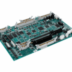
PCB Panel Utilization and Material Yield
Every board is cut from a panel, and the panel carries more than the boards it yields. Spacing, tooling, edge clearance and the way the array is singulated all consume area, and the difference between the area of the boards and the area of the panel is where cost is decided before the first process step.
What Panel Utilization Measures
Panel utilization is the ratio of finished board area to panel area, and it is usually quoted as a percentage. It is not the same as yield, because a board that is scrapped consumes panel area that was never going to be recovered, and it is not the same as material yield, which counts the laminate rather than the finished board.
The figure is worth tracking because it moves with design decisions that are made for other reasons. A small increase in edge clearance, or a change to the array spacing, shows up as a measurable cost rather than as an opinion. Our fabrication notes describe where those decisions are recorded.
Array Spacing and Singulation
The gap between boards in an array is set by the singulation method. A router needs a path for the cutter and a tab that the board can survive; a v-score needs a straight line and enough material each side of it; a laser or a punch needs its own allowance.
Each method takes area, and the method that takes the least area is often the one that puts the most stress on the board. Our breakaway tab notes set out how that trade is normally resolved without damaging the laminate or the joints.
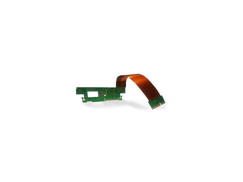
Edge Clearance and Tooling
The panel edge has to carry the tooling, which is usually a set of slots or holes that locate the panel in the drill and the conveyor. Copper is normally kept back from that edge so that the tooling does not touch a conductor, and the amount of material that is kept back is a direct subtraction from utilization.
Where the tooling is reused between products, the edge design can be standardised and the waste is predictable. Where every product has its own tooling, the edge has to be drawn afresh and is a common place for a tolerance to be missed.
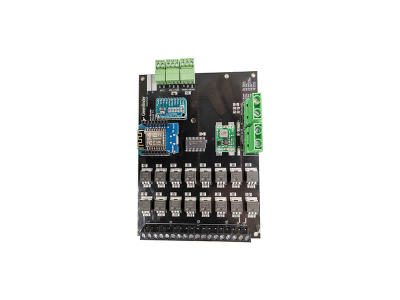
Panel Size and Equipment Limits
The panel has to fit the drill, the plating line, the lamination press and the assembly conveyor, and the smallest of those limits sets the maximum size. Within that limit, a larger panel is usually cheaper per board until an equipment constraint or a uniformity problem intervenes.
Uniformity is the reason the largest possible panel is not always the cheapest. Plating thickness, etch factor and temperature all vary across a large panel, and a board placed in the corner of an oversized panel can be outside the tolerance that the same board would hold near the centre.
Material Yield Versus Board Yield
Material yield counts how much of the purchased laminate becomes product, and it includes the panel that is rejected as well as the area that is cut away. A design with a high utilization and a high reject rate can consume more laminate than a design with a lower utilization and a stable process.
That is why the two figures are usually reported together. Improving utilization by tightening spacing can reduce laminate per board while increasing the scrap rate, and the net effect is only visible when both numbers are on the same page.
Warpage and Panel Support
A panel with an asymmetric array warps differently from a balanced one, because the copper and the laminate are not distributed evenly. Warpage costs yield in the assembly line rather than in the fabrication shop, and it is often the reason a change to the array is rejected after a trial.
Support in the reflow oven is part of the same question. A thin panel needs support that a thick one does not, and the support consumes space that the array would otherwise use. Our layer count notes describe how thickness and stack choice interact with that.
Copper Balance Across the Panel
Copper balance is judged across the panel rather than across the board, because the plating and the etch see the panel. A dense board placed next to a sparse one produces a local difference in current density that shows up as a thickness variation rather than as a visible defect.
Thieving and dummy pads can correct the balance, but they consume area, so they are part of the utilization calculation rather than a separate subject. Where they are added late, the array has to be re-drawn and the tooling re-quoted.
Records and Costing
Recording the panel size, the array count, the utilization and the material consumption per batch makes the costing reproducible. Without that record, a quotation for a repeat order is a guess, and the guess usually lands on the side that loses money.
The same record supports the design review. Where a change to edge clearance or spacing is proposed, the cost of the change is already on the sheet, and the decision can be made in a minute rather than in a meeting.
Process Control and Verification
On a design of this kind, copper balance is the item that decides how the rest of the board is arranged. Where the requirement is not written down, the shop supplies its own default, and the default is chosen for the process rather than for the design. The measurements that matter are the repeatable ones: conductor width and spacing, annular ring, finished hole size, plating thickness and surface finish are all verifiable on a coupon that travels with the panel.
Running a first article through the same checks as the production panel confirms that the two agree, and that comparison is the cheapest form of process control available at prototype stage. Keeping a sample from the panel turns a dispute into a measurement, because the same coupon can be re-examined by both parties without rebuilding the batch.
Process Control and Verification
On a design of this kind, copper balance is the item that decides how the rest of the board is arranged. Where the requirement is not written down, the shop supplies its own default, and the default is chosen for the process rather than for the design. The measurements that matter are the repeatable ones: conductor width and spacing, annular ring, finished hole size, plating thickness and surface finish are all verifiable on a coupon that travels with the panel.
Process Control and Verification
On a design of this kind, copper balance is the item that decides how the rest of the board is arranged. Where the requirement is not written down, the shop supplies its own default, and the default is chosen for the process rather than for the design. The measurements that matter are the repeatable ones: conductor width and spacing, annular ring, finished hole size, plating thickness and surface finish are all verifiable on a coupon that travels with the panel.
FAQ
Is a higher utilization always better? No. It is better when the process stays stable. A tighter array that raises scrap reduces the material saved by the tighter spacing.
Does the panel size affect the finished board? It can. Plating and etch uniformity vary across a panel, so the position of a board in the array affects what it measures.
What does gopcb provide for panel design? We provide array and spacing design against the singulation method, tooling that can be standardised between products, edge clearance that matches the equipment, utilization and material consumption reported per batch, and records that let a repeat order be quoted from data.