Parylene Coating for High Reliability PCB Assemblies
Most protective coatings are applied as a liquid, and every liquid shares the same limitations: it runs, it pools, it leaves thin spots over sharp edges and it cannot reach into the shadow behind a tall component. Parylene is different because it is not applied as a liquid at all. It is deposited from a vapour, one molecule at a time, which is why it covers geometry that no spray or dip can protect evenly.
What Makes Parylene Different
Parylene is a polymer that forms directly on the surface from a gaseous monomer. Because the material arrives as a gas and polymerises on contact, it does not depend on wetting, surface tension or gravity. The result is a thin, uniform, pinhole-free film that conforms to the exact shape of whatever it lands on.
The film is also chemically inert and has excellent dielectric properties, which makes it attractive for high impedance circuits and for sensors that must remain electrically stable in humid environments. Unlike a liquid conformal coating, there is no solvent to evaporate and no curing shrinkage, so the stress it applies to delicate features is minimal.
The Vacuum Deposition Process
Vacuum deposition happens in three stages inside a sealed chamber. The solid dimer is heated and vaporised, then passed through a pyrolysis furnace at around six hundred and eighty degrees Celsius, where it splits into a reactive monomer gas. That gas enters the deposition chamber, where it condenses and polymerises on every exposed surface at room temperature.
Because the process is a batch operation carried out under vacuum, parts are loaded on a rotating fixture to expose all sides. Rotation is not cosmetic: it determines whether the coating on a given face reaches the target thickness. Loading density also matters, since too many parts in the chamber consume monomer and produce a thinner coating than the recipe predicts.
Coverage of Edges, Holes and Fine Features
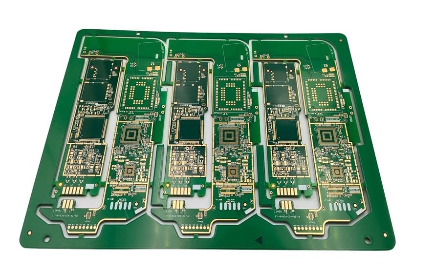
The vapour phase gives parylene a genuine advantage on difficult geometry. Sharp edges, wire bonds, the space under a component body and the inside of a small hole all receive a continuous film, subject to the reach of the gas. That reach is limited by line of sight in a practical sense, because the monomer must diffuse into a cavity before it polymerises.
Deep narrow gaps and the area directly beneath a large, closely seated component can therefore be shadowed. The film that forms there is thinner than on exposed surfaces, and in extreme cases it may be discontinuous. Evaluating a specific assembly usually means coating a sample and measuring the film in the most concealed location, not only on the accessible top surface.
Where Parylene Coating Is Used
The coating is common in medical devices, aerospace electronics, sensors and instrumentation, where reliability requirements justify the cost and the batch process. It is also used on flexible circuits, where its low modulus does not crack when the board bends, in contrast to some rigid liquid coatings.
It is less common in high volume consumer products because the vacuum batch process is slower and more expensive than spray coating, and because it cannot easily be applied selectively. Where the requirement is simply protection of a large, flat board, a liquid conformal coating is usually adequate. Parylene earns its place when geometry is difficult and the environment is demanding, as in the equipment discussed in this overview of industrial control electronics.
Masking and Rework Challenges
Parylene coats everything in the chamber, including connectors, test points, switches and optical surfaces. Masking is therefore extensive and often the most labour-intensive part of the job. Because the process is batch based, masking and demasking cost is repeated for every run, which is a significant part of the total expense.
Rework is the harder problem. The film is chemically resistant, so removing it locally requires mechanical abrasion, laser ablation or a specialised peel technique. Soldering through parylene is not possible without removing it first, and the removal process itself risks damaging the feature underneath. Designing the layout so that repairable and non-repairable areas are physically separated is a real advantage.
Comparison with Liquid Conformal Coating
A liquid conformal coating is applied by spray, brush or dip, cures in place and can be selectively applied with masking or dispensing. It is fast, well understood and cheap at scale, and modern materials offer good moisture resistance. Its weaknesses are edge coverage, thin spots over tall features and the tendency to bridge and trap solvent.
Parylene avoids those weaknesses at the cost of process complexity. It is also difficult to inspect optically because the film is transparent and very thin, which places more weight on process control and witness samples. Choosing between them is a question of geometry and environment rather than of absolute quality, and the comparison belongs alongside other manufacturing decisions in the PCB production flow.
Thickness, Testing and Quality Control
Typical parylene thicknesses range from a few micrometres for standard protection up to twenty-five micrometres or more for harsh environments. Thickness is controlled mainly by the amount of dimer charged into the chamber, so weighing the charge accurately is the primary process control. Coating thickness on witness coupons placed at different positions in the chamber verifies that the distribution is acceptable.
Additional checks include a tape adhesion test on a coated coupon and an insulation resistance measurement on a test pattern, both of which detect contamination or a deposition problem. Because the film is transparent, visual inspection is of limited value beyond confirming that the surface is covered and free of visible contamination.
Moisture Barrier and Dielectric Performance
Parylene is an excellent moisture barrier at typical coating thicknesses and maintains high surface and volume resistivity even after prolonged humidity exposure. That combination is why it is chosen for high impedance sensor circuits, where a small leakage current would destroy the measurement rather than merely degrade it.
Its dielectric strength is high and its dissipation factor is low, which makes the coating suitable for RF and high frequency assemblies where a lossy coating would change the circuit behaviour. The low dielectric constant relative to some liquid coatings also means less capacitive loading on sensitive traces, an effect worth checking on any impedance-controlled design.
Process Risks and Design Considerations
The main process risks are chamber loading errors, insufficient dimer, contamination on the parts before coating and shadowing in concealed areas. Cleanliness before deposition is critical, because the coating encapsulates whatever is on the surface rather than removing it. Ionic residue sealed under a parylene film is just as damaging as it would be without the coating.
Design considerations follow from the process. Provide clearance so the monomer can reach critical areas, avoid trapping air under components, keep connectors and test points accessible for masking, and specify the coating area precisely on the drawing. Building those requirements into the fabrication documentation, as discussed in this guide to PCB quality judgement, prevents most of the disputes that arise after coating.
FAQ
Is parylene coating better than liquid conformal coating? It is better for difficult geometry and harsh environments, because it deposits uniformly from vapour and does not suffer from edge thinning or pooling. Liquid coatings are faster, cheaper and easier to apply selectively, and they are adequate for many products. The right choice depends on the geometry, the environment and the volume.
Can parylene be removed for repair? Yes, but only by destructive methods such as abrasion, laser ablation or specialised chemical peel agents. There is no clean local removal that leaves the underlying feature untouched. Because of this, assemblies are usually designed so that any repairable feature sits outside the coated region and is masked during deposition.
How is the coating thickness verified? Thickness is primarily controlled by weighing the dimer charge and confirming the result on witness coupons placed at several positions in the chamber. Destructive measurement of a sample part gives a direct reading, and periodic insulation resistance testing on a coated test pattern confirms that the film is continuous and defect free.