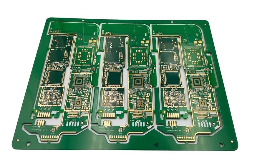
PCB Annular Ring: Drill Tolerance and Design Rules
Every plated hole in a board is surrounded by a ring of copper, and the width of that ring is one of the least glamorous and most consequential dimensions in the design. An annular ring that is too narrow breaks out of the pad, which can disconnect a layer, expose the laminate to plating chemistry and produce a joint that fails during thermal cycling.
What the Annular Ring Is
The annular ring is the copper remaining around a drilled hole after the hole is made. On an outer layer it is the pad minus the hole, expressed as the smallest width between the hole wall and the pad edge rather than as a diameter difference.
The minimum width occurs where the hole is offset from the pad centre, which happens because the drill position and the artwork are both subject to tolerance. The design rule therefore has to account for the worst case combination rather than for the nominal alignment.
Where the Tolerance Goes
Four tolerances combine. The artwork has a registration tolerance on each layer, the drill tolerance is expressed as a position tolerance relative to the panel, the hole itself has a diameter tolerance, and the pad is patterned with an etch tolerance that reduces its finished size.
The hole position tolerance is usually the largest of the four and is quoted by the fabricator for a given board thickness and drill size. A thinner board can be drilled more accurately than a thick one, and small holes are more difficult to place than large ones, so the achievable ring width depends on the rest of the design. That interaction is why the minimum ring is often quoted as a function of the aspect ratio rather than as a single number.

Outer and Inner Layer Rules
Outer layers are more forgiving because the pad can be made larger without any penalty other than space. A typical requirement is a minimum of fifty micrometres of ring on an outer layer for a general purpose board, with more for high reliability classes.
Inner layers are more constrained because a larger pad reduces the routing space around the via and can interfere with the plane clearance. The ring is also formed differently, since the inner layer is patterned before drilling and the copper is thinner. The rules for the clearance between a via and neighbouring copper on an inner layer are covered in the material on via to trace clearance in multilayer boards.

Breakout and Its Consequences
A breakout is where the hole extends beyond the pad so that no copper is left on one side. On an outer layer it appears as a crescent of exposed laminate and often as a broken connection to the track that joined the pad.
On an inner layer the consequences are more serious, because the breakout exposes the resin to the plating chemistry and may reduce the connection to the plane. A partial breakout can pass electrical test and fail later, since the remaining copper carries the current through a narrower section that is also more susceptible to thermal fatigue.
Teardrops and Their Use
A teardrop is a local widening of the pad where the track enters it, blending the two shapes. It increases the copper area around the connection and reduces the stress concentration where the track meets the pad, which improves resistance to thermal cycling and to mechanical handling.
Teardrops cost a small amount of routing space and are normally added automatically by the layout tool. They are particularly useful on pads that will be reworked or on vias in a flexible area, where the mechanical load is higher. Where a design is at the limit of its routing density, their value should be weighed against the space they consume rather than applied blindly.
Drill Size and Pad Size Selection
The pad size follows from the hole size plus the required ring on each side, plus an allowance for the etch tolerance that reduces the finished pad. Starting from a standard drill size and a standard pad size is the practical approach, because tooling is set up for those values and a non standard combination costs more.
The hole size itself should be the smallest that accepts the component lead or the via requirement with a reasonable clearance. A larger hole than necessary consumes pad area and reduces the available ring, while a hole that is too small makes insertion difficult and can damage a plated barrel during assembly. The pad geometry that results should follow the rules set out in PCB pad design standards.
Reliability Implications
The annular ring is part of the current path, and the copper around the barrel also provides the mechanical anchoring for the plating. A narrow ring reduces the cross section carrying the current into the layer and increases the stress in the copper when the board expands.
For a high reliability product, the ring is specified wider, and for a via that carries a large current it may be supplemented by additional vias rather than by a larger pad. The considerations are the same as those that govern via stack selection, where the structure of the connection is chosen for both the electrical and the mechanical requirement.
Verification
The ring is verified by microsection of a coupon from the panel, which shows the copper on each layer and the hole position. This is the only practical way to confirm that the process held the dimension, since the inner layers cannot be inspected optically.
For high reliability work, the measurement is recorded per panel and kept with the production records. Where a batch shows the ring at the low limit, the cause is usually a drift in the drill position or in the artwork registration, and both are process issues that are better corrected before the next order than after a field failure.
Design Practices
Keep the pad size consistent across similar holes so that the drilling programme and the panel design remain simple. Avoid placing the smallest pads next to the panel edge, where registration is hardest to hold, and give the drill programme a reasonable spread of hole sizes rather than many unique ones.
Where a via must sit in a dense area, the pad can be reduced only to the point where the ring requirement is still met, and no further. The temptation to shrink a pad to win routing space is the most common cause of a marginal board, and the space saved is rarely worth the yield that is lost. The wider set of decisions of this kind is described in PCB design guidelines for manufacturability.
FAQ
What is the minimum annular ring? Around fifty micrometres on an outer layer for a general purpose board, with wider requirements for high reliability classes and for thick boards with small holes.
Do vias need teardrops? They benefit from them, particularly in flexible areas or where thermal cycling is severe. The extra area is small compared with the reliability improvement.
Can a breakout be repaired? A minor outer layer breakout may be acceptable under the workmanship standard if the connection is intact. An inner layer breakout is not repairable and the panel is normally scrapped.