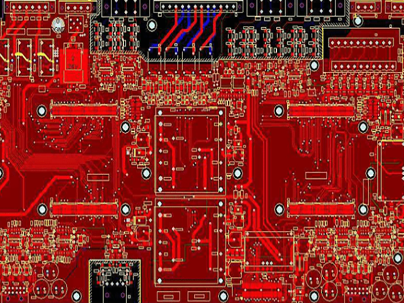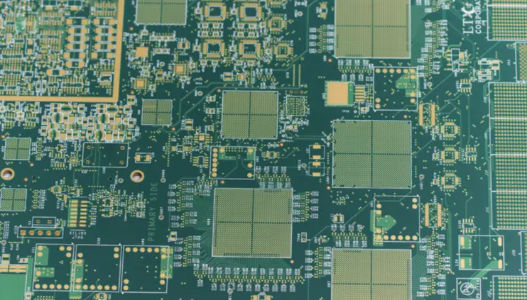
PCB Routing vs PCB Layout: What the Difference Really Means The two terms are used interchangeably in job listings and product descriptions, and the confusion causes real problems when a project is planned. Routing and layout are two phases of one process, and treating them as the same thing obscures…
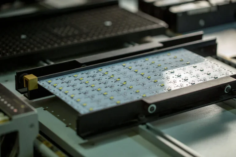
High Temperature PCB: Materials, Design and Applications Most boards spend their life near room temperature, and the design rules that follow from that assumption are built into every laminate datasheet. Move the operating temperature up and those assumptions weaken one by one: the laminate softens, expansion increases, solder joints see…
PCB Fiducial Placement Rules: Key Process and Quality Checks Modern electronics depend on boards that are assembled correctly the first time. Every product – a phone, a charger, a medical instrument or an industrial controller – relies on thousands of solder joints that must conduct current for years. This article…
PCB Solder Mask Bridge Over A Via: Key Process and Quality Checks Buyers and engineers often focus on the finished product and forget the production line behind it. In practice, most field failures can be traced back to process decisions made during assembly. Understanding PCB solder mask bridge over a…
Advanced HDI PCB Manufacturing: Stackups, Microvias and Yield Advanced HDI PCB manufacturing takes the density of a standard high density interconnect board one step further. Instead of one buildup layer on each side of a core, an advanced build stacks several laser drilled layers, uses via-in-pad structures under fine pitch…
Robot PCB Assembly: Vibration, Thermal and Inspection Requirements Robot PCB assembly is judged by whether the board still works after a year of movement. A joint that passes electrical test on the bench can crack when a servo reverses a hundred times a minute, and a driver stage that runs…
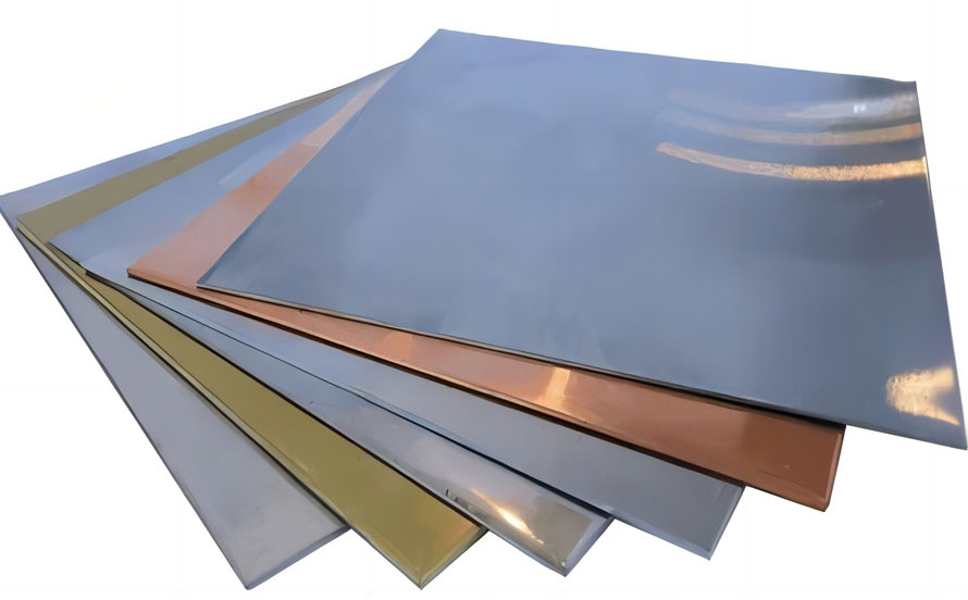
Special Process PCB Selection: Heavy Copper, HDI and Rigid-Flex Special process PCB work means going beyond the standard plated through hole multilayer build: heavier copper, laser drilled microvias, rigid-flex construction, metal core substrates, tight impedance control or cavity structures. Each of those processes adds cost and lead time, and each…
Redundant Layers in PCB Stackups: When an Extra Layer Pays Off A redundant layer is a copper layer that carries no dedicated circuit function in the first revision of a design. It is not a mistake and it is not waste. It is a deliberate allowance for routing growth, for…
Breadboard PCB: Soldered Prototyping Boards Compared A breadboard PCB sits between the solderless breadboard that engineers use for a first experiment and the fabricated board that goes into a product. It is a copper board laid out to mimic the connection pattern of a breadboard, so a circuit that was…
PCB Silkscreen Clarity Rules: What Buyers and Engineers Should Check Electronics manufacturing has become a discipline of small details. Solder paste volumes, placement accuracy, temperature profiles and inspection limits all add up to the final result. This guide looks at PCB silkscreen clarity rules from the perspective of a PCBA…