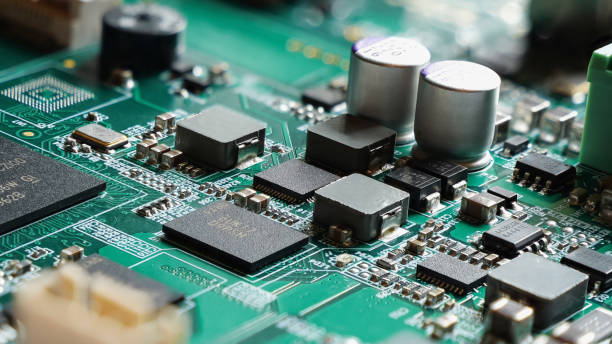
PCB Etch Back Process: Control, Stackups and Applications Etch back is a controlled removal of copper at the walls of a drilled or laser-formed hole. It prepares the inner-layer connection before plating, so the copper-to-copper joint forms cleanly. The process sits between drilling and plating, and its influence reaches far…
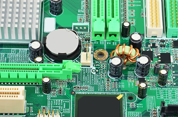
PCB Inner Layer Circuit Manufacturing Process Steps The inner layer circuit sets the electrical foundation of every multilayer board. Its quality shapes impedance behavior, layer registration, and long-term reliability of the finished product. As devices shrink and routing density rises, inner layer features must be produced with tighter consistency. The…
Carbon Ink PCB: Features, Process and Advantages Carbon ink printing adds a conductive layer directly onto the board surface. The ink forms contact pads and short conductive paths where metal would otherwise be plated or added. This approach suits keypads, membrane switches and low-current interfaces that see repeated pressing. Engineers…
RF PCB Lamination Structure Design Guide The lamination structure of an RF board sets how high-frequency signals travel from driver to receiver. Material choice, layer order, dielectric thickness and bond quality all shape loss, impedance and coupling. A stackup that looks acceptable on paper can still fail once the press…
Material Hardness and the PCB Manufacturing Process Material hardness rarely appears on a PCB drawing, yet it shapes how every panel moves through the factory. Substrates, copper foils, bonding films and solder masks each carry their own hardness, and each one reacts differently to cutting, drilling, etching and lamination. When…
Multilayer PCB Inner-Layer Lamination Sequence The inner-layer lamination sequence decides how well a multilayer board will behave. It fixes layer registration, cured dielectric thickness, residual stress and bond strength at the same time. For a routine four-layer or six-layer board the sequence is simple. For high-layer-count, mixed-material or high-speed products,…
HDI PCB vs Through-Hole PCB: Key Differences HDI boards and through-hole boards solve different problems, and the gap between them starts at the drill. One technology builds small vias through a few layers at a time. The other drills one hole through the whole board and plates it. That single…
Copper Foil Types in PCB Manufacturing Copper foil forms the conductive paths that carry every signal and every amp of current on a circuit board. The choice between electrolytic, rolled and ultra-thin foil changes impedance, bond strength, minimum trace width and final cost. It also changes how the fabrication house…
Small Batch Multilayer PCB Manufacturing Guide Small batch multilayer PCB manufacturing sits between prototype work and volume production. The lot may be a few dozen panels, yet the board still carries four or more layers, fine traces and controlled impedance. That combination removes the safety net of a long production…
PCB Storage Temperature Guidelines for Reliable Boards Boards leave the line in good condition, then sit in a warehouse for weeks. What happens during that wait decides whether the next assembly run meets its yield target. Temperature is the main variable in that window, because laminate, copper, solder mask and…