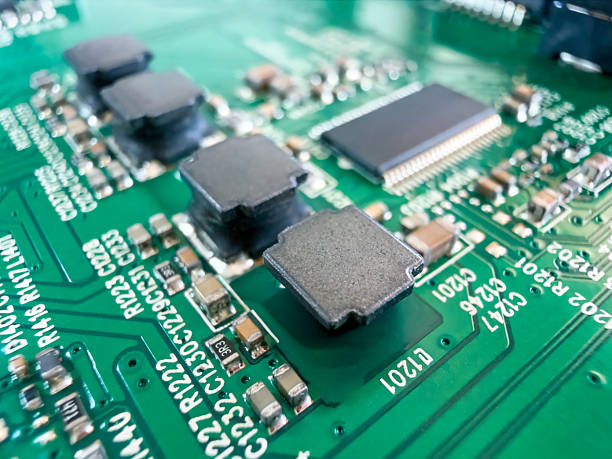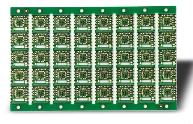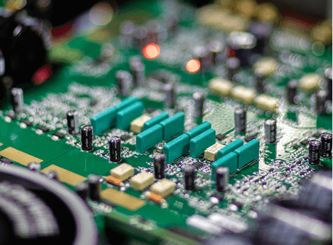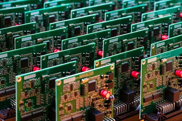
How to Test a PCB: PCB Testing Methods, Tools & Best Practices Printed circuit board manufacturing and assembly follow a detailed, controlled process in which every step must be completed accurately. However, even with strict process controls, manufacturing defects, assembly errors, and electrical problems can still occur. For this reason,…
1oz Copper PCB: 4-Layer Controlled Impedance Design A 1oz copper four-layer board sits at the practical center of high-speed design work. The copper weight gives useful current capacity and low conductor resistance. The four-layer stack gives designers two routing surfaces and two reference planes. Controlled impedance then ties the two…
PCB Corrosion: Causes, Types, How to Remove & Prevent PCB Corrosion PCB corrosion is the gradual deterioration of copper pads, solder joints, traces, and other metal components on a printed circuit board due to moisture, chemicals, contaminants, or other environmental factors. When metals such as copper and solder react with…
Millimeter-Wave PCB Design for 5G Small Cell Base Stations A 28 GHz small cell leaves little room for error. Signal loss climbs quickly with frequency, and a small change in dielectric thickness or copper roughness shifts impedance. The board inside the unit carries RF transmission, power amplification, frequency conversion and…
How to Detect a Short Circuit on a PCB: PCB Testing, Troubleshooting & Prevention Printed circuit boards (PCBs) have become essential components in almost every modern electronic product. As manufacturers continue to integrate more intelligent functions into individual devices, electronic circuits are becoming increasingly complex while simultaneously becoming smaller and…
Military-Grade vs. Industrial PCB: Key Differences, Cost & Performance In modern high-reliability electronic systems, the performance of a printed circuit board (PCB) directly determines whether hardware can run stably in harsh environments. Both defense-grade PCBs and industrial PCBs belong to the high-reliability circuit production domain. However, they differ much in…
10-Layer 1.6mm Controlled Impedance PCB Guide A ten-layer board at 1.6mm finished thickness gives high-speed designs room for dedicated signal, power and ground layers. Controlled impedance ties that stack-up to predictable transmission-line behavior. The combination suits networking gear, optical modules, radar units and dense computing boards. This guide explains the…
16-Layer PCB at 5.0mm: Ultra-Thick Board Guide A 16-layer board built to 5.0mm overall thickness is not a standard catalog item. It combines a high layer count with a stack height that changes how every process behaves. Drilling gets deeper, lamination gets harder, and plating must reach further into each…
Automotive PCB in EVs, ADAS & Powertrain With the rapid advancement of new energy vehicles (EVs), Advanced Driver Assistance Systems (ADAS), and smart powertrain systems, car electronics have placed unprecedented demands on the performance and reliability of auto-grade PCBs. Unlike consumer devices, car electronic systems must run stably for 10–15…
2.5 Mil Fine Line PCB Manufacturing for Dense Electronics A 2.5 mil trace is about 0.0635 mm wide. That single number changes how a board must be built, inspected and quoted. Fine lines let engineers pack more connections into a small footprint, but they also shrink the process window at…