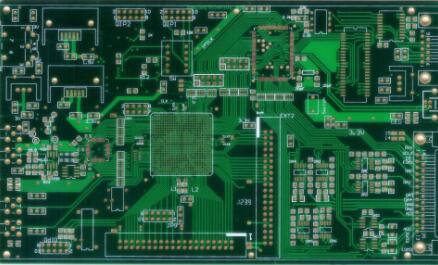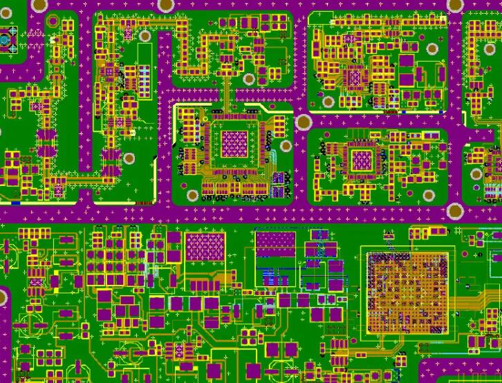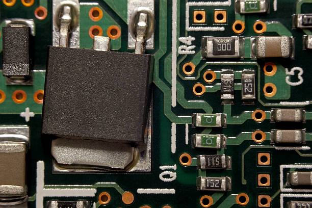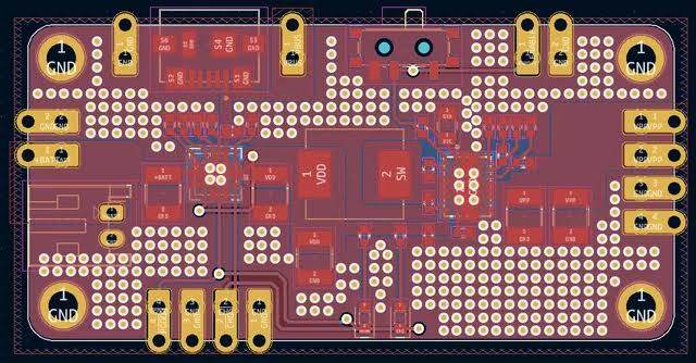
HDI PCB technology represents one of the most advanced directions in modern printed circuit board manufacturing. As electronic products continue to become smaller, lighter, and more highly integrated, conventional PCB structures are increasingly unable to meet the requirements for fine-pitch components, dense routing, and compact interconnections. By combining finer circuit…
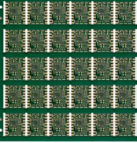
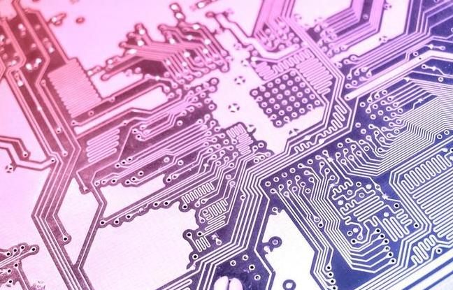
As HDI PCB technology continues to evolve alongside highly integrated ICs and high-density interconnect technology, it has become one of the most important developments in modern PCB fabrication. HDI technology enables finer lines, smaller microvias, higher wiring density, and more compact board structures, particularly for smartphones and other miniaturized electronic…
As electronic systems continue to operate at higher speeds and frequencies, high-frequency PCB design has become increasingly important for achieving stable signal transmission, reliable power delivery, and good electromagnetic compatibility. High-frequency and high-speed PCB designs are more sensitive to trace geometry, layer stack-up, power distribution, return-current paths, component placement, and…
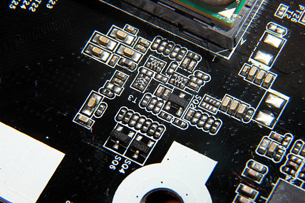
As electronic products continue to evolve toward miniaturization, higher performance, and greater integration, SMT assembly has become one of the most important technologies in modern electronics manufacturing. Compared with traditional through-hole assembly, surface mount technology offers significant advantages in component density, electrical performance, production efficiency, automation, and overall manufacturing cost.…
PCB Copper Thickness Control in Fabrication Copper thickness decides how much current a trace can carry and how much heat it sheds. It also affects resistance, voltage drop and long-term reliability in the field. Control is not a single step on the line. It runs through deposition, etching, surface finishing…
How to Achieve ±0.2mil Trace Width and Spacing Control A ±0.2mil tolerance on trace width and spacing sits close to the practical limit of conventional imaging and etching. It is not won by one machine. It comes from the way material, imaging, etching, environment and inspection are held together across…
Solder Mask Process Explained for PCB Builds Solder mask sits on the finished board as a thin green layer, yet it decides how well the board solders and how long it survives. The process behind that layer covers surface preparation, coating, alignment, curing and inspection. Each step leaves a mark…
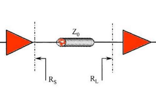
In high-speed PCB design, PCB impedance matching is an important technique for maintaining signal integrity and reducing signal reflections, overshoot, ringing, and electromagnetic interference. As signal rise times become faster and transmission distances increase, PCB traces can no longer always be treated as simple electrical connections. Instead, they may behave…
Scaling High-Density and Miniaturized PCB Production Small boards with dense layouts move through a fab differently from simple boards. Scaling high-density and miniaturized PCB production means the process must hold tighter windows on every panel, not just the first one. Thin cores, fine traces and small vias leave little room…
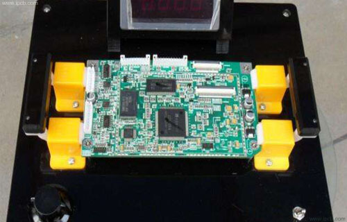
During PCB assembly, accurate temperature control is essential for achieving reliable solder joints and preventing defects. To obtain an accurate temperature profile, thermocouples are commonly attached to selected points on the PCB and monitored as the board passes through the reflow oven. For solder paste printing and subsequent reflow soldering,…